High temperature microelectromechanical (MEM) devices and fabrication method

a microelectromechanical and fabrication method technology, applied in the field of microelectromechanical (mem) devices, can solve the problems of metallization layer, aluminum-based metallization layer, and device failure in this manner, and achieve the effects of reducing the number of microelectromechanical devices

Active Publication Date: 2007-12-04
TELEDYNE SCI & IMAGING
View PDF14 Cites 20 Cited by
  • Summary
  • Abstract
  • Description
  • Claims
  • Application Information

AI Technical Summary

Problems solved by technology

However, devices fabricated in this manner may fail if subjected to high temperatures.
If the fluid temperature is high, the device's organic adhesive can degrade and compromise the device's structural integrity.
In addition, the metallization layer, typically aluminum-based, may also be adversely affected by exposure to high temperature fluids.

Method used


Image

  • High temperature microelectromechanical (MEM) devices and fabrication method
  • High temperature microelectromechanical (MEM) devices and fabrication method
  • High temperature microelectromechanical (MEM) devices and fabrication method

Examples


Embodiment Construction

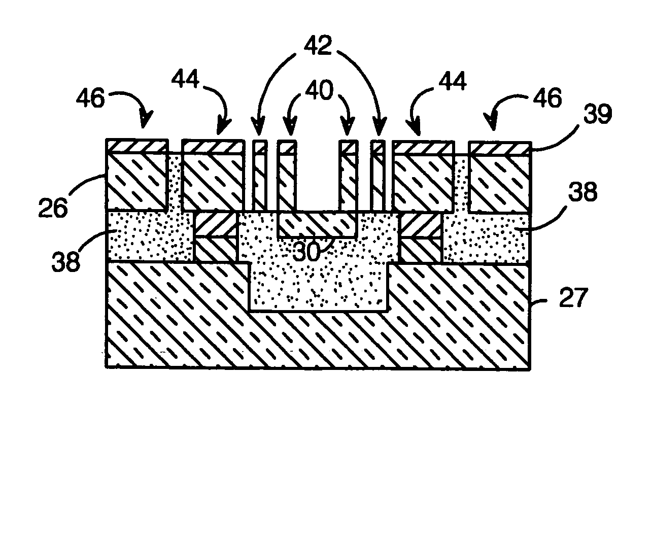
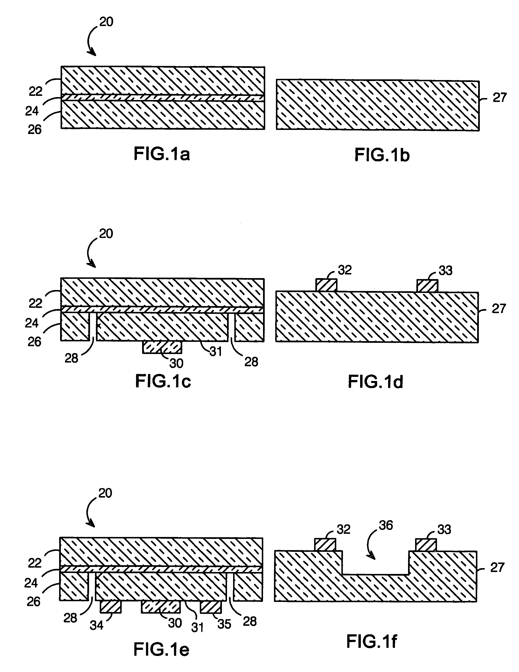
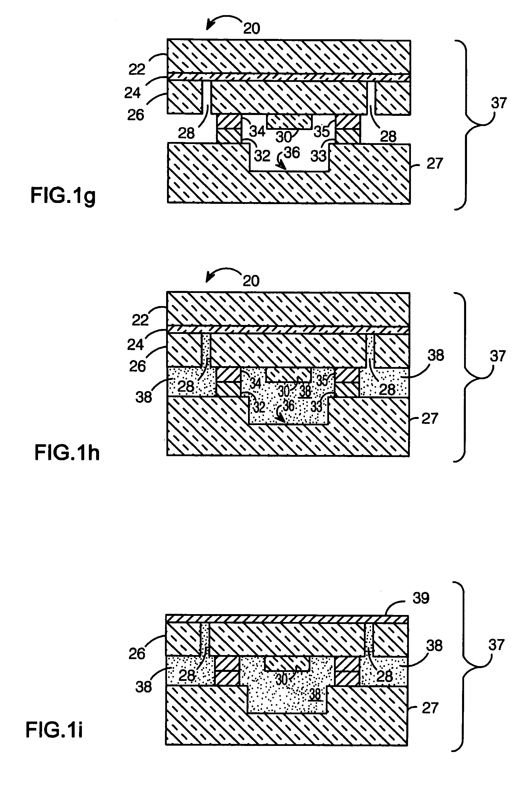
[0016]The present invention is directed to MEM devices and a fabrication method for making same that enables the devices to withstand higher temperatures than similar devices fabricated using prior art methods. Epoxy and metallization that might degrade under high temperature conditions are replaced with a high temperature bonding material and refractory metals, greatly extending the range of temperatures over which MEM devices such as a viscosity sensor can operate without failing.

[0017]In general, MEM devices per the present invention have a stationary element and a movable element displaceable relative to the stationary element. Each device comprises a semiconductor wafer—preferably an SOI wafer, a substrate—which can be insulating or conductive, and a high temperature bond which bonds the wafer to the substrate to form a composite structure. Portions of the composite structure are patterned and etched to define the stationary and movable MEM elements such that the movable elemen...


PUM

PropertyMeasurementUnit
temperaturesaaaaaaaaaa
pressureaaaaaaaaaa
temperatureaaaaaaaaaa

Abstract

A microelectromechanical (MEM) device per the present invention comprises a semiconductor wafer—typically an SOI wafer, a substrate, and a high temperature bond which bonds the wafer to the substrate to form a composite structure. Portions of the composite structure are patterned and etched to define stationary and movable MEM elements, with the movable elements being mechanically coupled to the stationary elements. The high temperature bond is preferably a mechanical bond, with the wafer and substrate having respective bonding pads which are aligned and mechanically connected to form a thermocompression bond to effect the bonding. A metallization layer is typically deposited on the composite structure and patterned to provide electrical interconnections for the device. The metallization layer preferably comprises a conductive refractory material such as platinum to withstand high temperature environments.

Description

BACKGROUND OF THE INVENTION[0001]1. Field of the Invention[0002]This invention relates to the field of microelectromechanical (MEM) devices, and particularly to methods of fabricating MEM devices for use in high temperature environments.[0003]2. Description of the Related Art[0004]Microelectromechanical (MEM) devices—i.e., integrated devices which include at least one moveable element that moves relative to a stationary element—have become commonplace. Such devices have found many applications, including switches, tunable capacitors, current sensors, viscosity sensors, accelerometers and the like.[0005]One approach to fabricating MEM devices, described, for example, in U.S. Pat. No. 6,159,385 and U.S. Patent Application Publication U.S. 2004 / 0113513, involves the use of a silicon-on-insulator (SOI) wafer and a substrate. The SOI wafer, which includes a layer of doped silicon and an oxide layer, is bonded to the substrate using an organic adhesive to form a composite structure. The d...

Claims


Application Information

Patent Timeline
Patent Type & Authority Patents(United States)
IPC IPC(8): H01L21/00
CPCB81C1/0069B81C2203/032
Inventor DENATALE, JEFFREY F.BORWICK, III, ROBERT L.STUPAR, PHILIP A.
Owner TELEDYNE SCI & IMAGING
Why Eureka
Try Eureka