Method for determining the depth of a buried structure

a technology of buried structure and depth, applied in the direction of optical radiation measurement, instruments, spectrometry/spectrophotometry/monochromators, etc., can solve the problems of complex and laborious methods, high cost, and destruction of wafers, and achieve non-destructive, cost-effective and fast results

Inactive Publication Date: 2007-12-11
POLARIS INNOVATIONS LTD
View PDF16 Cites 14 Cited by
  • Summary
  • Abstract
  • Description
  • Claims
  • Application Information

AI Technical Summary

Benefits of technology

[0009]The present invention provides a nondestructive, cost-effective and fast method for determining the depth of a buried structure in a semiconductor wafer.
[0011]This method enables nondestructive determination of the depth of a buried structure in a semiconductor wafer, so that costs and also time can be saved. At the same time, the method can be applied to a product wafer and can be carried out directly after a process for fabricating the buried structure.
[0019]In order to carry out this method, a customary ellipsometer is preferably used, by means of which changes in the state of polarization of radiation reflected at a sample can be determined simply and without any problems.
[0020]The invention uses electromagnetic radiation having wavelengths in the infrared range for irradiating the semiconductor wafer. With the aid of this radiation, in contrast to radiation having wavelengths in the optically visible range, it is possible to determine the depth of a structure in the region of a number of μm, since this radiation is distinguished by low absorption and thus a high penetration depth in the semiconductor wafers, essentially composed of silicon. Moreover, the radiation used suppresses scattering effects at the buried structure and thus lateral details which can adversely influence the determination of the depth, since the wavelengths of the radiation, lying approximately in the range of 2 to 20 μm, are significantly greater than the lateral dimensions of the buried structure, which are to be established approximately in the region of 100 nm. As a result of this, the semiconductor wafer, on account of a material change brought about by the buried structure, acts as an apparently homogeneous layer system with different refractive indices at which reflection takes place.

Problems solved by technology

However, this method turns out to be complicated and laborious due to the required breaking of the semiconductor wafer.
Furthermore, the semiconductor wafer is destroyed by being broken, as a result of which the method is extremely cost-intensive.
Furthermore, since the method cannot be applied to the product wafers which continue in production, deviations may occur between the measured depth of a structure and the depth of a corresponding structure of a product wafer.

Method used


Image

  • Method for determining the depth of a buried structure
  • Method for determining the depth of a buried structure
  • Method for determining the depth of a buried structure

Examples


first embodiment

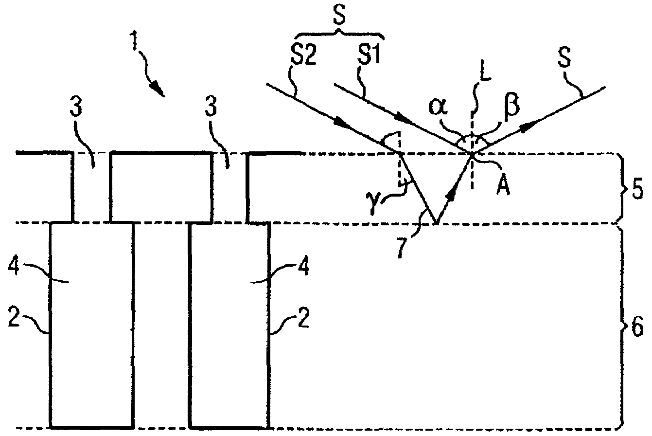
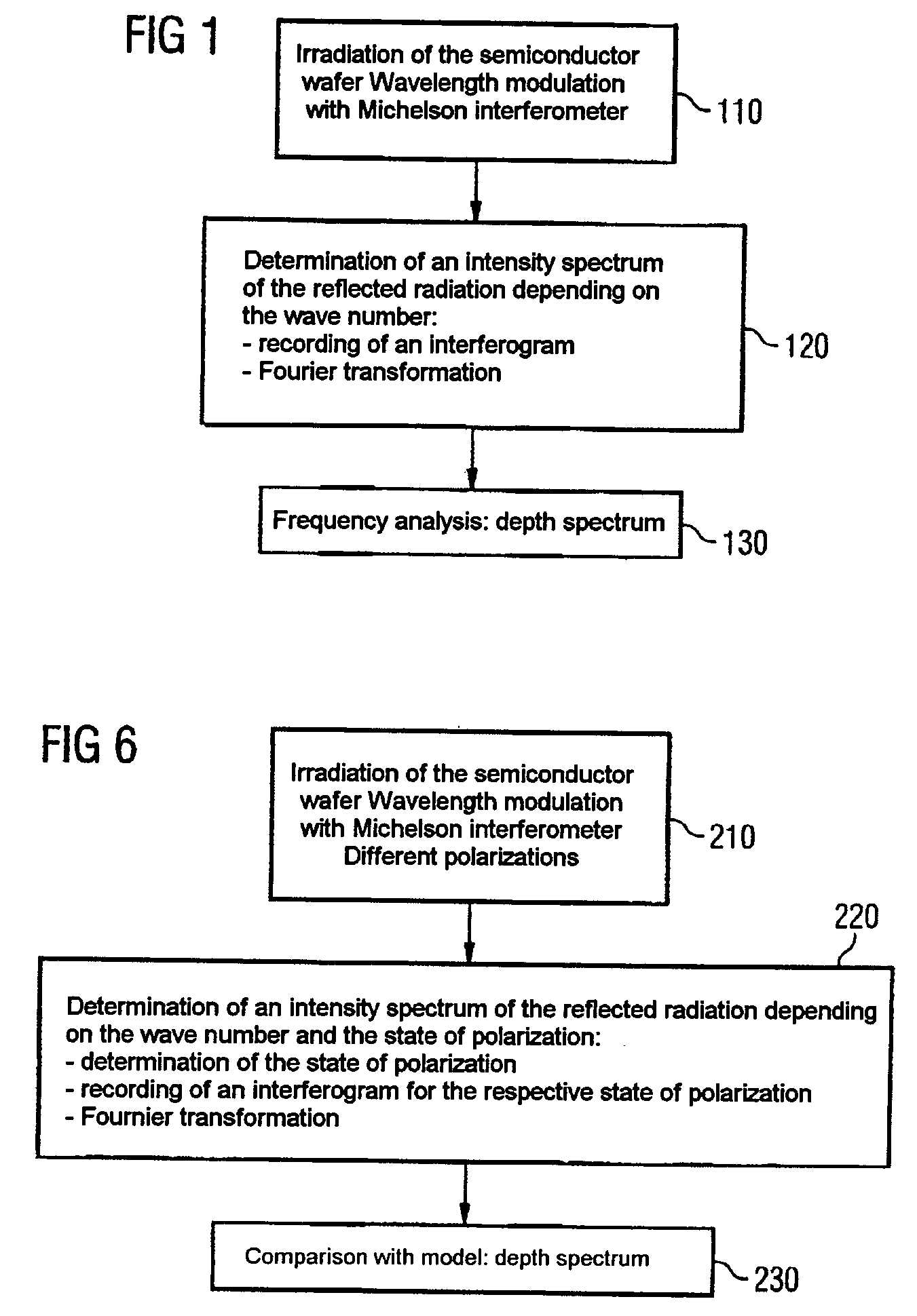
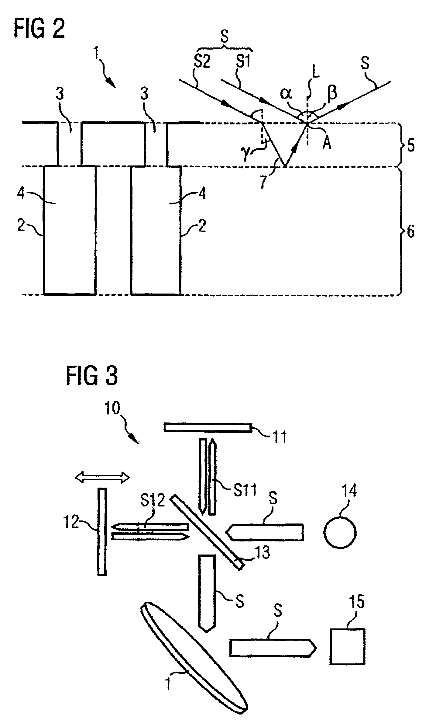
[0036]FIG. 1 shows a flow diagram of a method according to the invention for determining the depth of a buried structure in a semiconductor wafer. For this purpose, in 110, the semiconductor wafer is irradiated at a predetermined angle of incidence with respect to a surface of the semiconductor wafer with electromagnetic radiation in a wavelength range, the wavelengths used lying in the infrared range and being modulated in a frequency-dependent manner with the aid of a Michelson interferometer. In this case, the modulation of the wavelengths is dependent on the position of a movable mirror of the Michelson interferometer.

[0037]In 120, an intensity spectrum of the reflected radiation is determined depending on the wave number of the wavelength range of the radiated-in electromagnetic radiation at an angle of reflection—corresponding to the angle of incidence—with respect to the surface of the semiconductor wafer. Stepp 120 can be split into two substeps. In a first substep, the inte...

second embodiment

[0059]FIG. 6 shows a flow diagram of a method according to the invention. In this case, in 210, the semiconductor wafer is irradiated at a predetermined angle of incidence with respect to a surface of the semiconductor wafer with electromagnetic radiation in the infrared range, the wavelengths again being modulated in a frequency-dependent manner with the aid of a Michelson interferometer. The radiation is additionally oriented in different polarization directions or states of polarization.

[0060]Step 220 involves determining an intensity spectrum of the radiation reflected at the surface of the semiconductor wafer depending on the wave number and the state of polarization, which is altered by the reflection. Step 220 can be subdivided into three substeps. A first substep involves determining the state of polarization of the reflected radiation. A second substep involves recording an interferogram for the respective state of polarization and a third substep involves converting this i...

third embodiment

[0065]The determination of the depth of a buried structure in a semiconductor wafer can also be effected by means of an angle-dependent intensity spectrum with respect to a predetermined wavelength, instead of a wave-number-dependent intensity spectrum. In this respect, FIG. 8 shows a flow diagram of a method according to the invention.

[0066]In this case, in 310, the semiconductor wafer is irradiated at different angles of incidence or a continuously tuned range of angles of incidence with respect to a surface of the semiconductor wafer with electromagnetic radiation having a predetermined wavelength lying in the infrared range, and in 320 involves recording an intensity spectrum of the radiation reflected at the semiconductor wafer at angles of reflection corresponding to the angles of incidence with respect to the surface of the semiconductor wafer.

[0067]An intensity spectrum determined in this way depending on the angles of reflection includes information about constructive and d...


PUM

PropertyMeasurementUnit
wavelengthsaaaaaaaaaa
depthaaaaaaaaaa

Abstract

The present invention relates to a method for determining the depth of a buried structure in a semiconductor wafer. According to the invention, the layer behavior of the semiconductor wafer which is brought about by the buried structure when the semiconductor wafer is irradiated with electromagnetic radiation in the infrared range and arises as a result of the significantly longer wavelengths of the radiation used in comparison with the lateral dimensions of the buried structure is utilized to determine the depth of the buried structure by spectrometric and / or ellipsometric methods.

Description

CLAIM FOR PRIORITY[0001]This application claims the benefit of priority to German Application No. 103 19 843.1, filed in the German language on May 3, 2003, the contents of which are hereby incorporated by reference.TECHNICAL FIELD OF THE INVENTION[0002]The present invention relates to a plurality of methods for determining the depth of a buried structure in a semiconductor wafer.BACKGROUND OF THE INVENTION[0003]Electronics is dominated nowadays by microelectronic components with integrated circuits. Such integrated circuits comprise a complex arrangement of electronic structures which are interconnected in a plurality of planes arranged one above the other on a common semiconductor substrate, also referred to as chip. The fabrication of these circuits is characterized by a complicated succession of different process steps.[0004]One of the principle requirements of the semiconductor industry is the continuous increase in performance as a result of ever faster circuits, which is link...

Claims


Application Information

Patent Timeline
Patent Type & Authority Patents(United States)
IPC IPC(8): G01B11/02G01B11/22G01J3/453G01N21/21
CPCG01B11/22G01N21/211G01J3/453
Inventor HECHT, THOMASSCHRODER, UWEMANTZ, ULRICHJAKSCHIK, STEFANORTH, ANDREAS
Owner POLARIS INNOVATIONS LTD
Why Eureka
Try Eureka