Plasma display panel
a technology of display panel and plasma, which is applied in the direction of discharge tube luminescnet screen, instrument, electrode, etc., can solve the problems of increasing the voltage for maintaining a discharge, increasing the abrasion of the front panel electrode, and time delay phenomenon, so as to increase brightness and efficiency, the effect of reducing the amount of erroneous discharge in each cell
- Summary
- Abstract
- Description
- Claims
- Application Information
AI Technical Summary
Benefits of technology
Problems solved by technology
Method used
Image
Examples
first embodiment
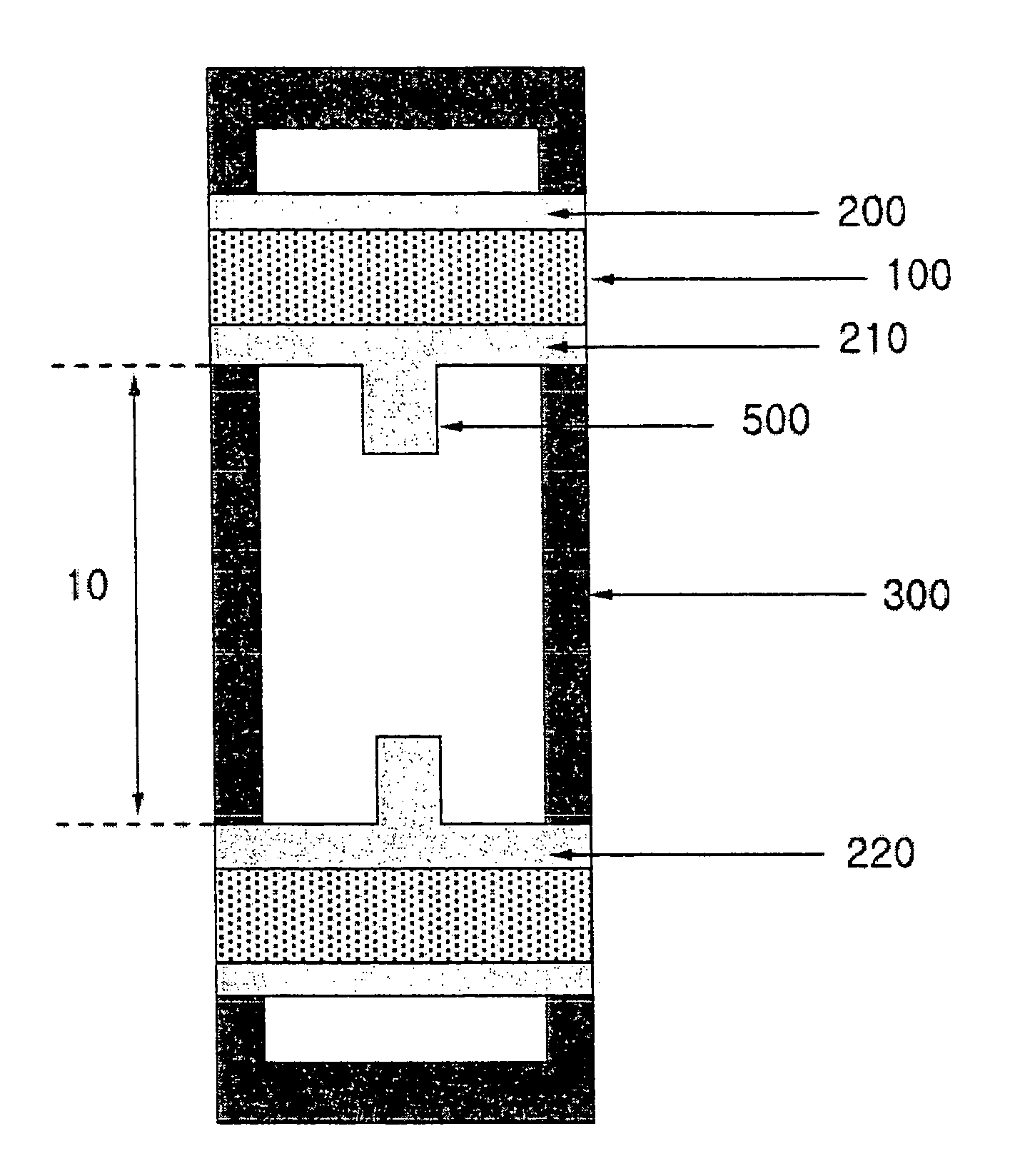
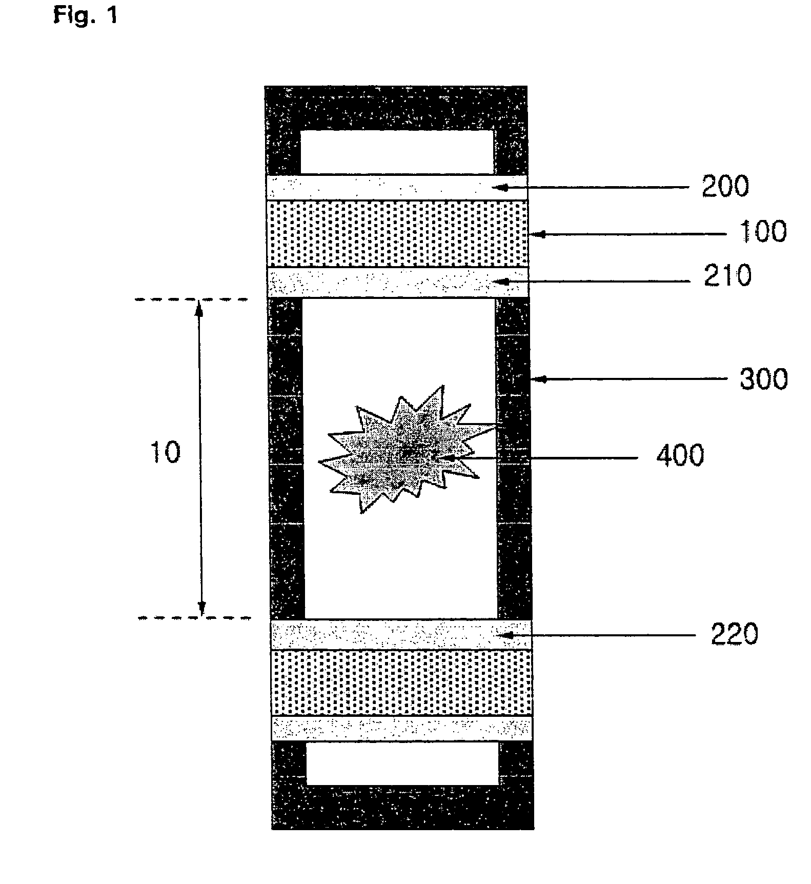
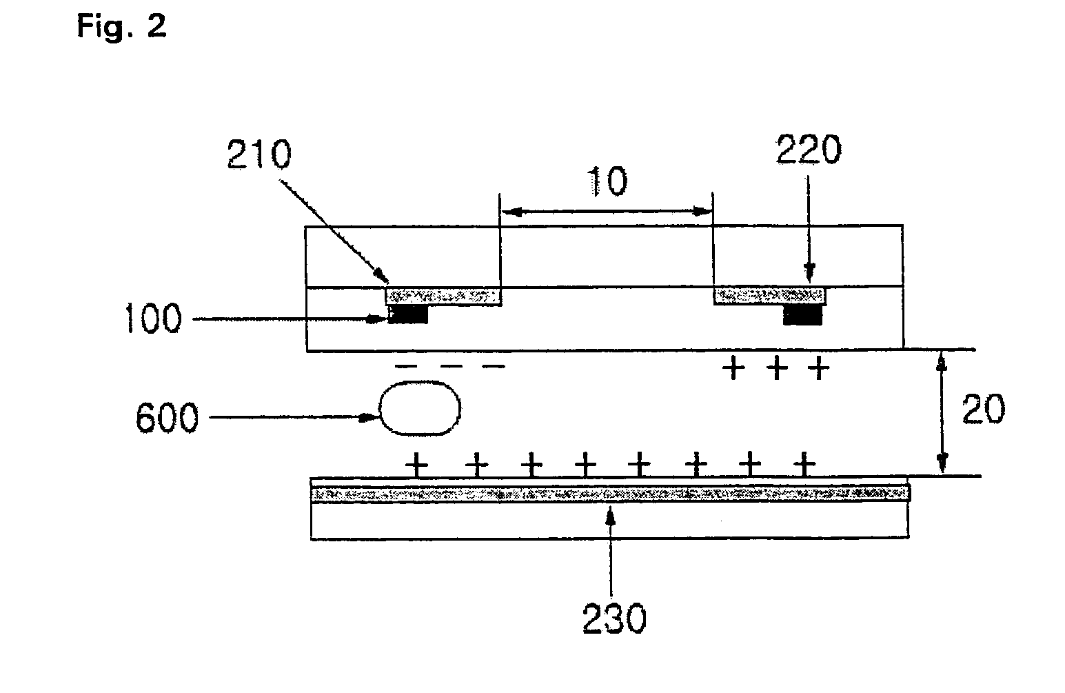
[0040]A plasma display panel according to a first embodiment of the present invention includes a front substrate and a rear substrate that are opposite to each other, wherein the plasma display panel includes scan electrodes and sustain electrodes that are spaced apart from each other in parallel on the opposite surface of the front substrate and have transparent electrodes and metal electrodes, respectively, a dielectric layer that covers the scan electrodes and the sustain electrodes, a protection film coated on the dielectric layer, address electrodes formed on the opposite surface of the rear substrate, a dielectric layer that covers the address electrodes, barrier ribs formed on the dielectric layer, discharge cells demarcated by the barrier ribs, and a phosphor layer coated on the inside of the discharge cells, wherein a distance between the scan electrodes and the sustain electrodes is greater than that between the front substrate and the rear substrate, wherein the transpare...
second embodiment
[0058]A plasma display panel according to a second embodiment of the present invention includes a front substrate and a rear substrate that are opposite to each other, wherein the plasma display panel includes scan electrodes and sustain electrodes that are spaced apart from each other in parallel on the opposite surface of the front substrate and have transparent electrodes and metal electrodes, respectively, a dielectric layer that covers the scan electrodes and the sustain electrodes, a protection film coated on the dielectric layer, address electrodes formed on the opposite surface of the rear substrate, a dielectric layer that covers the address electrodes, barrier ribs formed on the dielectric layer, discharge cells demarcated by the barrier ribs, and a phosphor layer coated on the inside of the discharge cells, wherein a distance between the scan electrodes and the sustain electrodes is greater than that between the front substrate and the rear substrate, wherein the transpar...
third embodiment
[0076]A plasma display panel according to a third embodiment of the present invention includes a front substrate and a rear substrate that are opposite to each other, wherein the plasma display panel includes scan electrodes and sustain electrodes that are spaced apart from each other in parallel on the opposite surface of the front substrate and have transparent electrodes and metal electrodes, respectively, a dielectric layer that covers the scan electrodes and the sustain electrodes, a protection film coated on the dielectric layer, address electrodes formed on the opposite surface of the rear substrate, a dielectric layer that covers the address electrodes, barrier ribs formed on the dielectric layer, discharge cells demarcated by the barrier ribs, and a phosphor layer coated on the inside of the discharge cells, wherein a distance between the scan electrodes and the sustain electrodes is greater than that between the front substrate and the rear substrate, wherein floating tran...
PUM
 Abstract
Description
Claims
Application Information


