Power FET with embedded body pickup

a technology of power transistors and pickups, applied in the field of power transistors, can solve the problems of limiting the amount of reducing the spacing “d” in certain fabrication processes, shortening the contact, and affecting the quality of the transistor,

Active Publication Date: 2008-01-01
MICREL
View PDF9 Cites 134 Cited by
  • Summary
  • Abstract
  • Description
  • Claims
  • Application Information

AI Technical Summary

Problems solved by technology

However, as fabrication technology moves toward smaller dimensions and the use of tungsten plug contacts, shorting contacts, which typically have to be made bigger than the minimally sized contacts, are disfavored or not allowed entirely in certain fabrication processes.
However, in conventional fabrication processes, the need to include the body contact diffusion region 60 in the source regions limits the amount of reduction in spacing “d” that can be made.
Thus, the necessity of forming the body pickup contact limits the amount of reduction of spacing “d” in power transistor 10 even as technology scales down.
Another difficulty in the manufacturing of the power transistor 10 of FIG. 2 is the source / drain mask 30 used to block out the source / drain implants to areas where the body contact diffusion regions are to be formed.
However, it is generally more difficult to form small islands of photoresist.
Small islands of photoresist may not be properly exposed and may be lifted off during the developing process.
Furthermore, it is difficult to maintain the integrity of small photoresist islands when the photoresist islands are subjected to high energy ion bombardment, such as when the patterned photoresist is used for the source / drain implantation step.
During the high energy ion bombardment of the ion implantation process, small islands of photoresist are susceptible to degradation, causing the photoresist to be lifted off and redeposited as resist dust, contaminating the substrate.
Although the power transistor operates functionally, the ruggedness of the power transistor is compromised when there are insufficient body pickup contacts.
Currently, there is no reliable way to detect lifted-off or peeled off photoresist islands, as these islands exist in numbers of thousands or millions in the source / drain mask.

Method used


Image

  • Power FET with embedded body pickup
  • Power FET with embedded body pickup
  • Power FET with embedded body pickup

Examples


Embodiment Construction

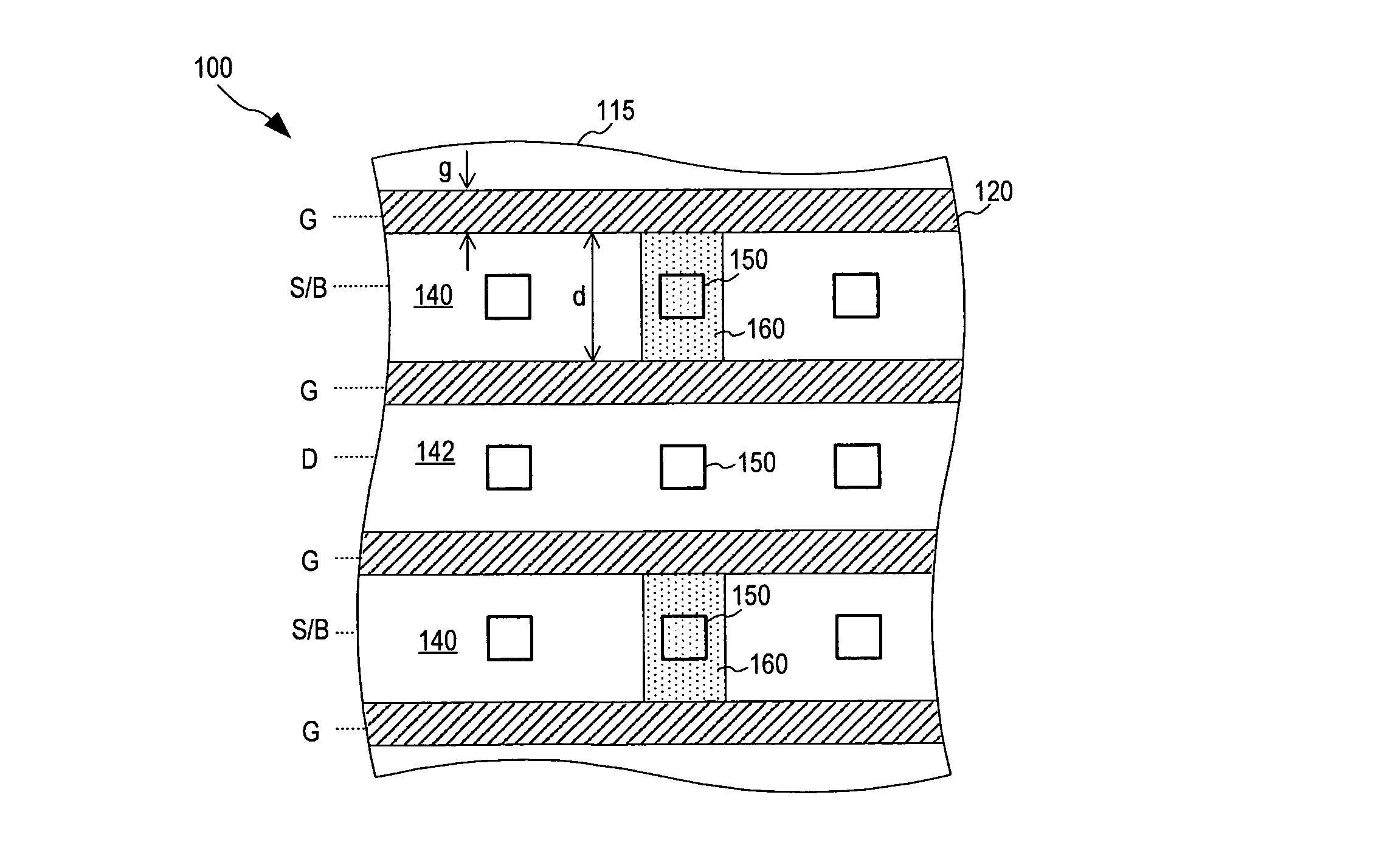
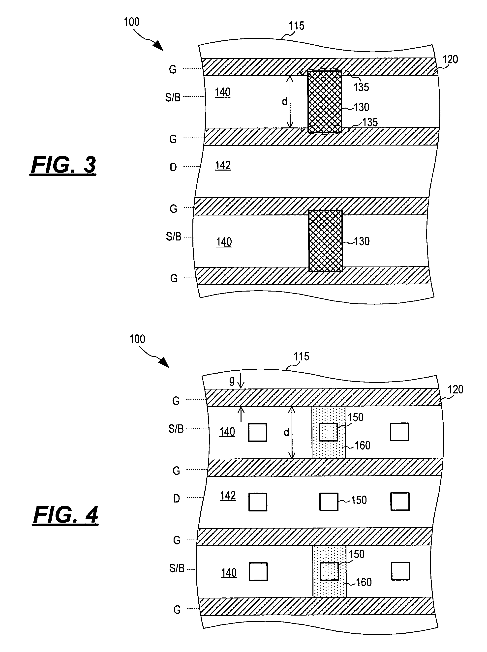
[0021]In accordance with the principles of the present invention, a power field effect transistor (FET) includes embedded body pickup contacts that are formed over body contact diffusion regions that extend to the two adjacent minimally spaced polysilicon lines. By elongating the body contact diffusion region, the source / drain implant mask includes elongated islands of photoresist defining the body contact diffusion regions where the elongated photoresist islands improve the manufacturability and production worthiness of the power transistor. Meanwhile, the power FET of the present invention can achieve high power efficiency by minimizing the spacing between two polysilicon lines while improving the reliability and ruggedness of the power transistor. Specifically, the spacing between two polysilicon lines can be kept at the minimal distance dictated by the fabrication process so that the area of the transistor and the term Ron*Area are minimized to improve power efficiency.

[0022]In ...


PUM


Abstract

A power transistor formed on a semiconductor substrate and including a lateral array of polysilicon lines separated by alternating source and drain regions includes one or more body contact diffusion regions formed in the source regions where each body contact diffusion region has a length that extends to the edges of the two adjacent polysilicon lines, and one or more body pickup contacts where each body pickup contact is formed over a respective body contact diffusion region. In one embodiment, the body contact diffusion regions are formed in a fabrication process using ion implantation of dopants of a first type through a body diffusion mask. Each body contact diffusion region defined by an exposed area in the body diffusion mask has a drawn area that overlaps the respective two adjacent polysilicon lines.

Description

FIELD OF THE INVENTION[0001]The invention relates to power transistors and, in particular, to a power transistor with embedded body pickup contacts for improved ruggedness while maintaining small device size.DESCRIPTION OF THE RELATED ART[0002]Power transistors or power field effect transistors (FET) are well known semiconductor devices. One type of power transistors is a lateral power transistor formed as an array of transistors. Other power transistor structure includes vertical power transistors. In a lateral power transistor structure, an array of polysilicon lines forms the gate terminal with alternating drain and source regions disposed between the polysilicon lines. The body of the power transistor, having an opposite dopant type to the source / drain regions, can include the substrate and / or one or more diffusion regions (e.g., a well region) in which the source and / or drain regions of the power transistor are formed.[0003]In a power transistor, it is necessary to make an ohmi...

Claims


Application Information

Patent Timeline
Patent Type & Authority Patents(United States)
IPC IPC(8): H01L29/76
CPCH01L29/1083H01L29/4175H01L29/78
Inventor ALTER, MARTIN
Owner MICREL
Why Eureka
Try Eureka