
Technique to reduce ESD loading capacitance

a technology of esd and loading capacitance, applied in the direction of emergency protective circuit arrangement, emergency protective arrangement for limiting excess voltage/current, transistor, etc., can solve the problems of reducing the protection level of esd, affecting the quality of esd input/output signals, and reducing the capacitance. , to achieve the effect of reducing esd capacitance, maintaining necessary esd protection levels, and reducing capacitan

Inactive Publication Date: 2008-01-01
SEIKO EPSON CORP
View PDF16 Cites 20 Cited by
  • Summary
  • Abstract
  • Description
  • Claims
  • Application Information

AI Technical Summary

Benefits of technology

[0017]To achieve these objects, a capacitive reduction circuit is placed between an electrostatic-protection diode and a power rail. One end of the electrostatic-protection diode is coupled to an input signal and its other end is coupled to the capacitive reduction circuit at a junction node. The capacitive reduction circuit applies a compensation voltage to this junction node whose value is selected to assure that a reverse bias is maintained across the electrostatic-protection diode during normal (i.e. non-ESD) operation. By maintaining a reverse bias across the electrostatic-protection diode, its capacitive loading effect can be maintained to a predefined maximum. To assure that a reverse bias is maintained, the compensation voltage is made to be of greater magnitude than the power rail.
[0019]In one embodiment, the capacitive reduction circuit includes a voltage generator for providing the compensation voltage at the junction node. Preferably, the output from the voltage generator is applied to the junction node through a current steering diode, which mitigates the flow of current from the junction node to the voltage generator.

Problems solved by technology

Therefore, an ESD circuit adds substantially to the loading capacitance on a pad, and this has a detrimental effect on high frequency input / output signals.
However, this approach tends to degrade the ESD protection level, which typically needs to be greater than 2000 V.
Further complicating the use of ESD protection circuits in high frequency applications is that it has been shown that the junction capacitance of a diode is related to the voltage applied across the diode.
The use of differential amplifiers, however, limits its use in high frequencies applications.
This approach, furthermore, does not address the issue of reducing the capacitance of clamping diodes 13 and 15.

Method used


Image

  • Technique to reduce ESD loading capacitance
  • Technique to reduce ESD loading capacitance
  • Technique to reduce ESD loading capacitance

Examples


Embodiment Construction

[0046]Preferred embodiments of the present invention are described below with reference to the accompanying figures.

[0047]The present invention is described in connection with various preferred embodiments thereof with reference to the accompanying drawings. However, various changes and modifications will be apparent to those skilled in the art based on the foregoing description. Such changes and modifications are intended to be included within the scope of the present invention to the extent they fall within the scope of the appended claims.

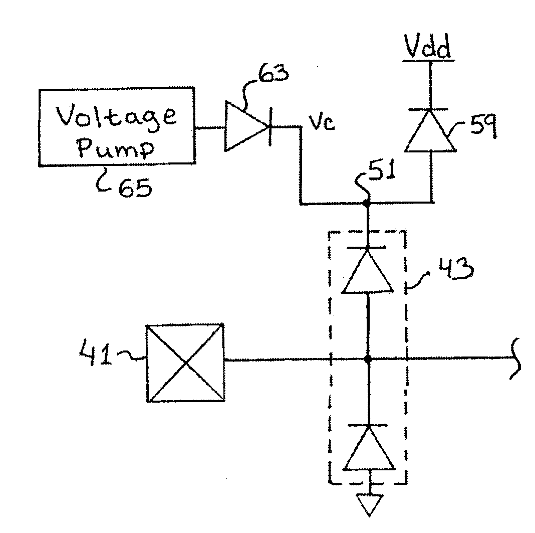
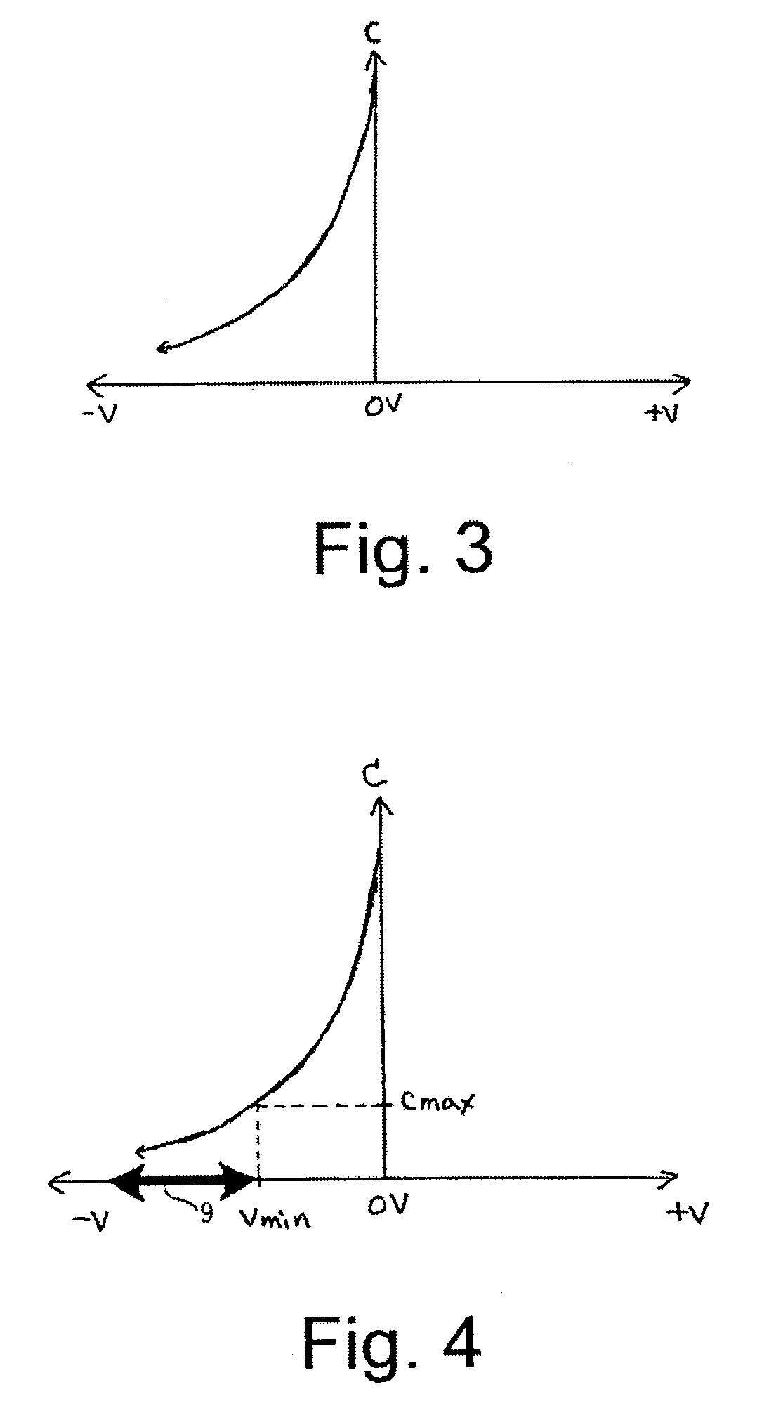
[0048]It has been shown that the capacitance across a diode can be affected by an applied reverse bias potential. The relationship between a diode's capacitance and an applied reverse bias potential may be expressed as,

Cj(Vj)=Cj(0V){1−Vj / Vbi}−n

where Vj is the junction voltage, Cj(Vj) is the resulting capacitance per unit area, Cj(0V) is the capacitance at Vj=0V, Vbi is the junction built-in potential, and n represents the power dependence of cap...


PUM


Abstract

The capacitive loading effects of an ESD circuit having an electrostatic-protection diode are reduced by using a capacitance compensation circuit. Under normal operation when no electrostatic discharge is experienced, the capacitance reduction circuit maintains a reverse bias across the electrostatic-protection diode, which causes the diode's capacitance to be reduced below a predetermined value. When an electrostatic discharged is experienced, the capacitance compensation circuit removes the applied reverse bias, and shunts the electrostatic-protection diode to a power rail.

Description

BACKGROUND OF THE INVENTION[0001]1. Field of the Invention[0002]The present invention relates generally to the field of electrostatic discharge (ESD) protection for high frequency applications.[0003]2. Description of the Related Art[0004]The input impedance of a MOSFET, and some other devices, is capacitive making it inclined to build electrostatic charges. Thus, even a small amount of static charge placed on a bonding pad connected to a gate, from something or someone external to the MOSFET chip, can accumulate on the input capacitive impedance and build up to become a large enough electric field to cause the gate oxide of the MOSFET to break down.[0005]An electrostatic discharge (ESD) circuit, or device, is typically applied to input, output, and input / output pads of a semiconductor integrated circuit (IC), or other sensitive device, to protect internal circuitry from electrostatic discharge, both in the manufacturing process and post-manufacturing handling.[0006]With reference to...

Claims


Application Information

Patent Timeline
Patent Type & Authority Patents(United States)
IPC IPC(8): H02H9/00H01L21/822H01L27/04H01L21/8238H01L27/02H01L27/06H01L27/092
CPCH01L27/0255
Inventor HARGROVE, MICHAELPETROSKY, JOSEPH
Owner SEIKO EPSON CORP
Features
  • Generate Ideas
  • Intellectual Property
  • Life Sciences
  • Materials
  • Tech Scout
  • Unparalleled Data Quality
  • Higher Quality Content
  • 60% Fewer Hallucinations
Learn More