Coating and developing apparatus and coating and developing method

a technology of coating and developing apparatus, applied in the direction of photosensitive materials, fishing, instruments, etc., can solve the problems of reducing the yield, affecting the yield, and the transfer program becomes extremely complicated, so as to suppress the reduction of the yield of substrates

Active Publication Date: 2008-01-29
TOKYO ELECTRON LTD
View PDF8 Cites 32 Cited by
  • Summary
  • Abstract
  • Description
  • Claims
  • Application Information

AI Technical Summary

Benefits of technology

[0015]Accordingly, it is an object of the present invention to provide a coating and developing apparatus, and a coating and developing method, which can perform an ordinary process on a substrate in a process block when an abnormality occurs in a transfer mechanism which transfers substrates to and from an exposure apparatus, thereby suppressing reduction in the yield of substrates.
[0074]According to the present invention, when an abnormality occurs in the second transfer mechanism intervened between the process block and the exposure apparatus, the first transfer mechanism in the unit block for coating-film formation is controlled in such a way that those substrates which are present in that unit block for coating-film formation retreat to the first substrate retaining section after an ordinary process is performed in the unit block for coating-film formation, and transfer of any substrate into the unit block for coating-film formation is inhibited. Accordingly, even when an abnormality occurs in the second transfer mechanism, the unit block for coating-film formation can finish a scheduled process on a substrate in the unit block. Therefore, any substrate will not be left remaining in each unit in the unit block, such as a liquid process unit or a heating unit, thereby preventing the quality of the coating film from being degraded as a consequence of the otherwise possible case where a next process cannot be performed at a set timing.

Problems solved by technology

As the transfer program is complex, if the transfer devices 15a and 15b are allowed to retreat in the transfer path, the transfer program becomes extremely complicated, which is not practical.
If a wafer W is left remaining in a module this way, various problems occur.
A wafer W left inside each module often hardly meets a predetermined quality, in which case the wafer cannot be delivered as a product, thus reducing the yield.
When some kind of abnormality occurs in the transfer mechanism provided in the interface block, therefore, the aforementioned problem may come up.

Method used


Image

  • Coating and developing apparatus and coating and developing method
  • Coating and developing apparatus and coating and developing method
  • Coating and developing apparatus and coating and developing method

Examples


Embodiment Construction

[0092]A preferred embodiment of the present invention will now be described referring to the accompanying drawings.

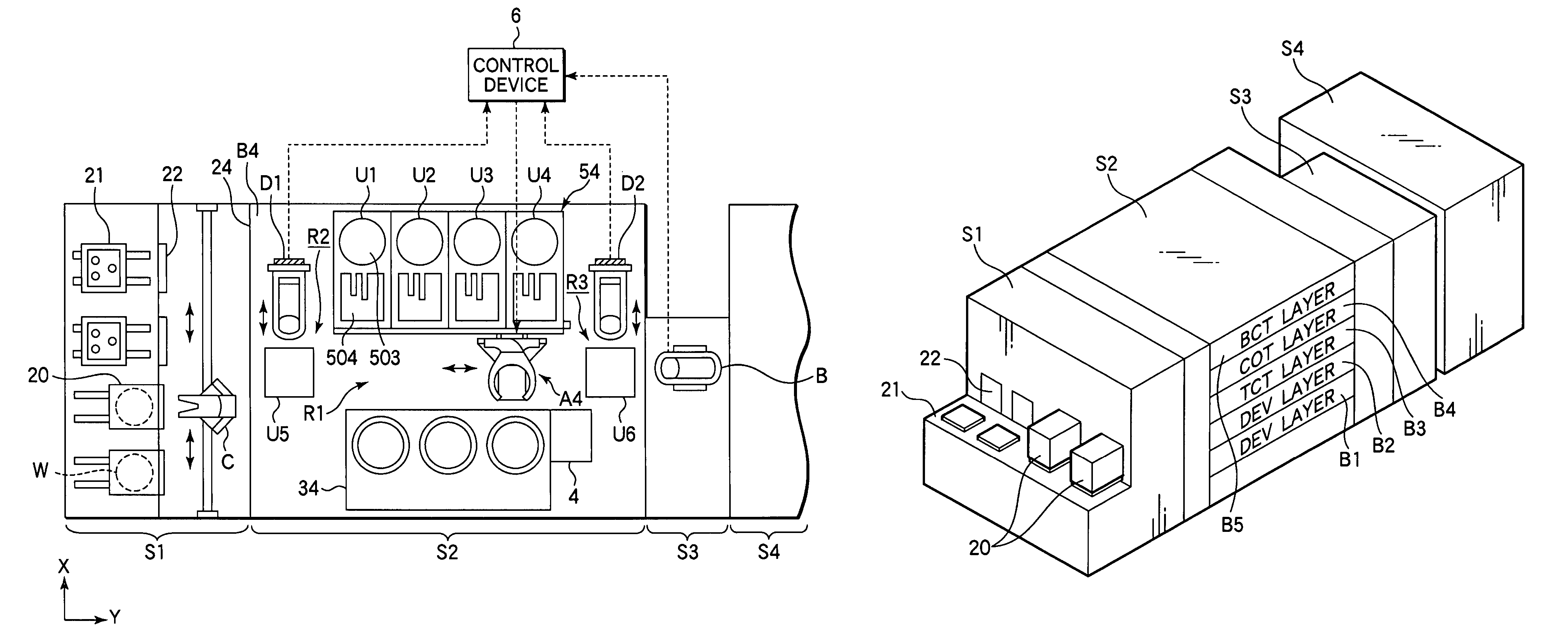
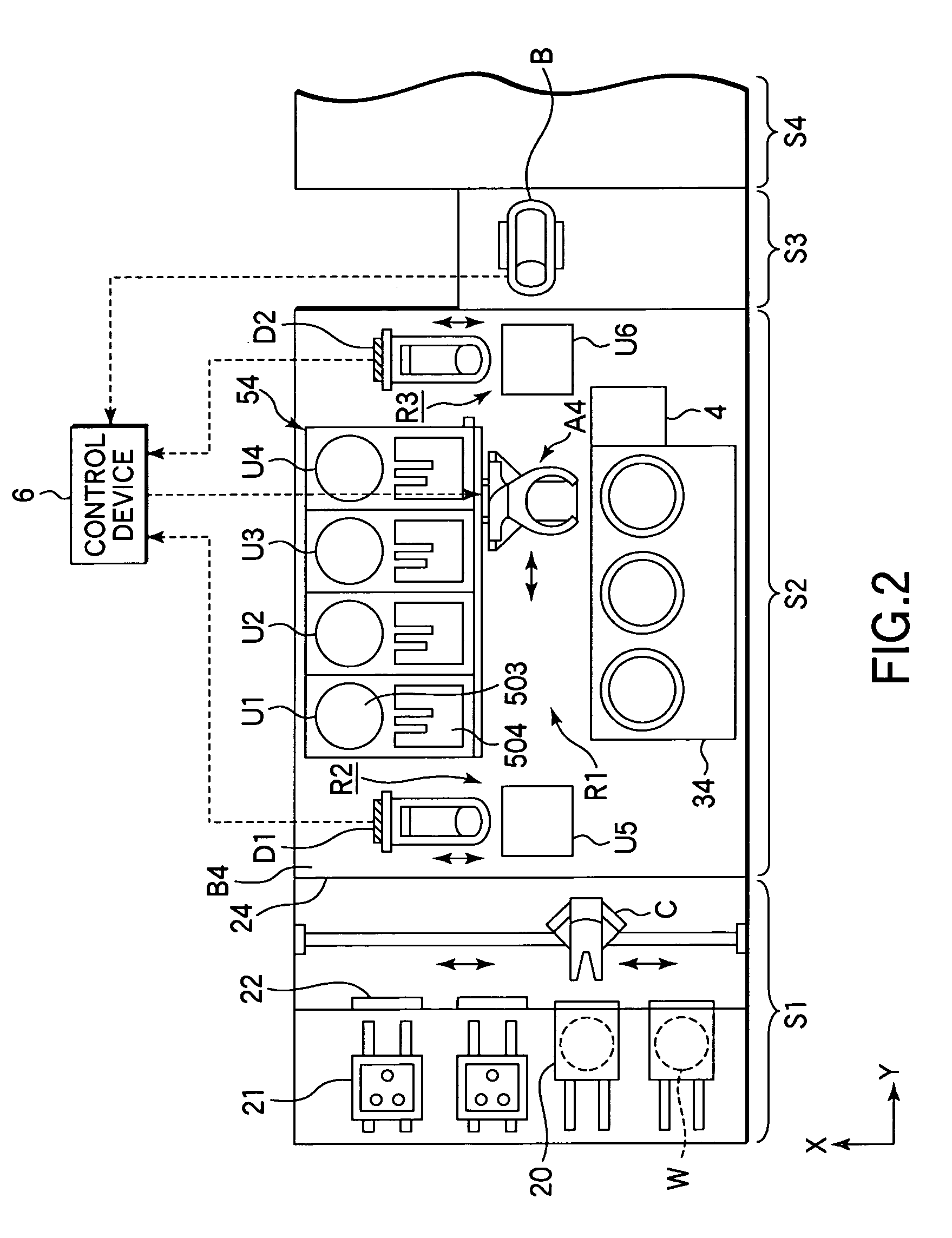
[0093]FIG. 2 is a plan view showing a resist pattern forming apparatus equipped with a coating and developing apparatus according to one embodiment of the present invention, FIG. 3 is a schematic perspective view of the coating and developing apparatus, and FIG. 4 is a schematic side view of the coating and developing apparatus. The coating and developing apparatus comprises a carrier block S1 which carries in and out carriers 20 each retaining, for example, thirteen wafers W or substrates in an airtight manner, a process block S2 provided adjacent to the carrier block S1 and having five unit blocks B1 to B5, and an interface block S3 provided on the opposite side of the process block S2 to the carrier block S1. The resist pattern forming apparatus has an exposure apparatus S4 connected to the interface block S3. The operation of the resist pattern forming apparatus is ...


PUM


Abstract

A coating and developing apparatus comprises a process block which forms a resist film on a wafer, then transfers the wafer to an exposure apparatus, and performs a developing process on the wafer after exposure, and an interface transfer mechanism provided between the process block and the exposure apparatus. The process block includes unit blocks for coating-film formation and unit blocks for development laid out in a stacked manner. When an abnormality occurs in the interface transfer mechanism, an ordinary process in the unit block for coating-film formation is performed on those substrates which are present in that unit block for coating-film formation, after which processed wafers are retreated to a retaining unit and transfer of any wafer into the unit block for coating-film formation is inhibited.

Description

BACKGROUND OF THE INVENTION[0001]1. Field of the Invention[0002]The present invention relates to a coating and developing apparatus, and a coating and developing method, which perform a coating process of applying a resist liquid or the like to a substrate, such as a semiconductor wafer or a glass substrate for liquid crystal display (LCD substrate), and a developing process on the substrate after exposure.[0003]2. Description of the Related Art[0004]In a fabrication process of a semiconductor device or an LCD substrate, a resist pattern is formed on a substrate using a technology called photolithography. According to the technology, a resist liquid is applied to the top surface of a substrate, such as a semiconductor wafer, to form a liquid film, which is then dried to be a resist film, the resist film is exposed into a desired pattern using a photomask, and then a developing process is performed to yield a resist pattern corresponding to the exposure pattern.[0005]Such a sequence ...

Claims


Application Information

Patent Timeline
Patent Type & Authority Patents(United States)
IPC IPC(8): G03D5/00
CPCH01L21/67173H01L21/67178H01L21/67276H01L21/67754A01K93/00A01K91/03
Inventor AKIMOTO, MASAMIHAYASHI, SHINICHIHAYASHIDA, YASUSHIMATSUOKA, NOBUAKI
Owner TOKYO ELECTRON LTD
Why Eureka
Try Eureka