
Method for tuning epitaxial growth by interfacial doping and structure including same

a technology of interfacial doping and growth rate, applied in the direction of semiconductor devices, basic electric elements, electrical appliances, etc., can solve the problems of insufficient simultaneous growth, excessive thinning of the underlying crystalline or polycrystalline surface from which the epitaxial film is grown, etc., to achieve the same growth rate prevent the growth of an epitaxial material in that surface region

Inactive Publication Date: 2008-02-12
GLOBALFOUNDRIES INC
View PDF3 Cites 0 Cited by
  • Summary
  • Abstract
  • Description
  • Claims
  • Application Information

AI Technical Summary

Benefits of technology

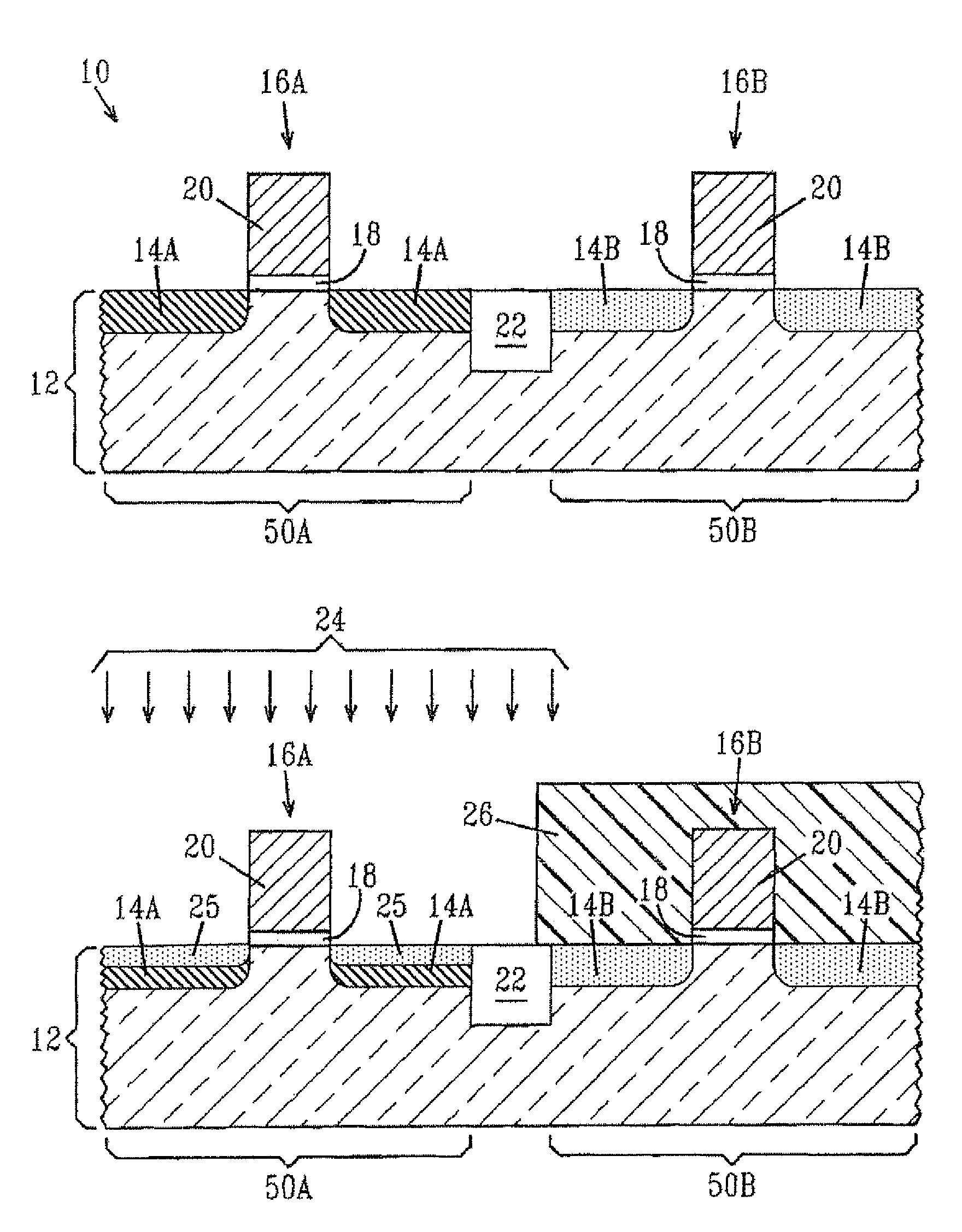
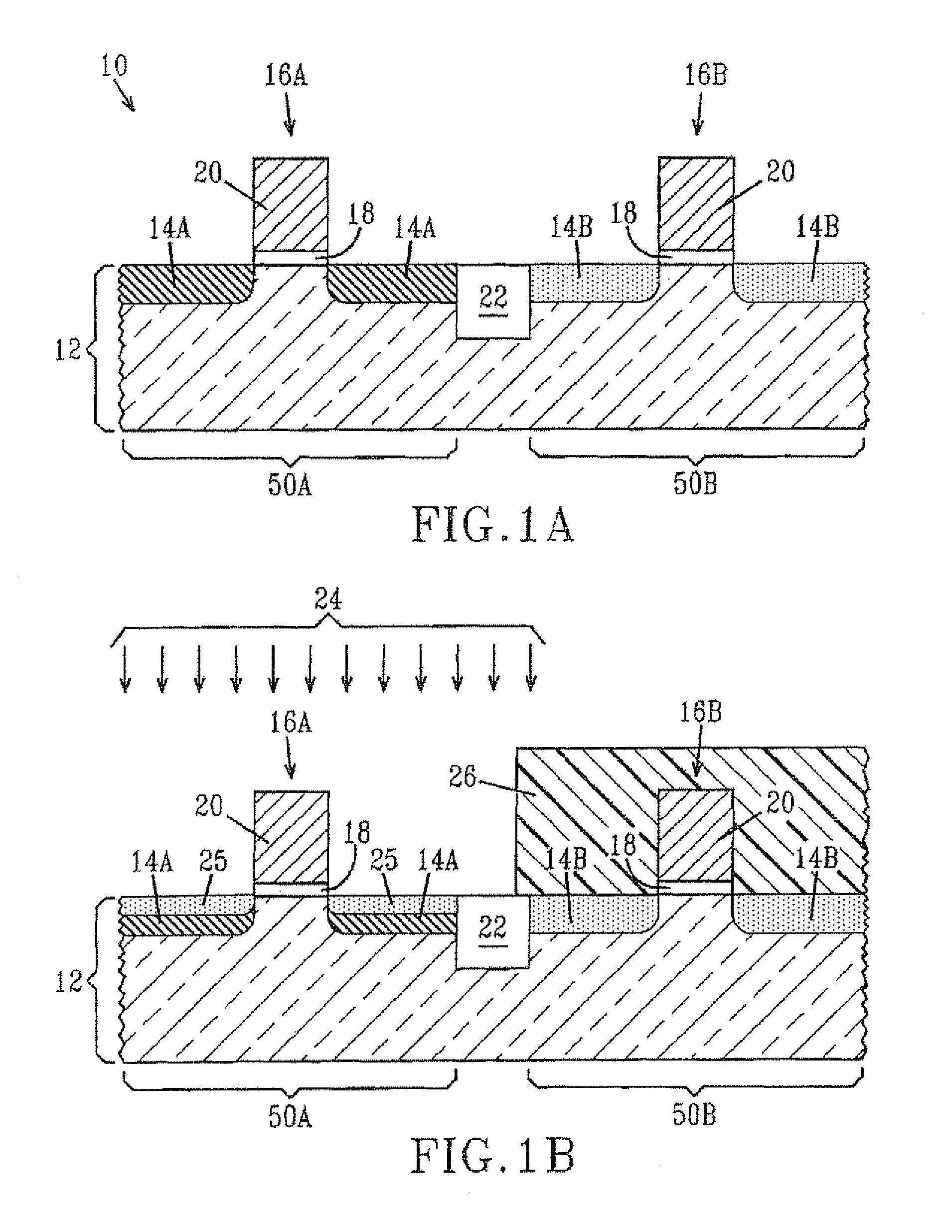
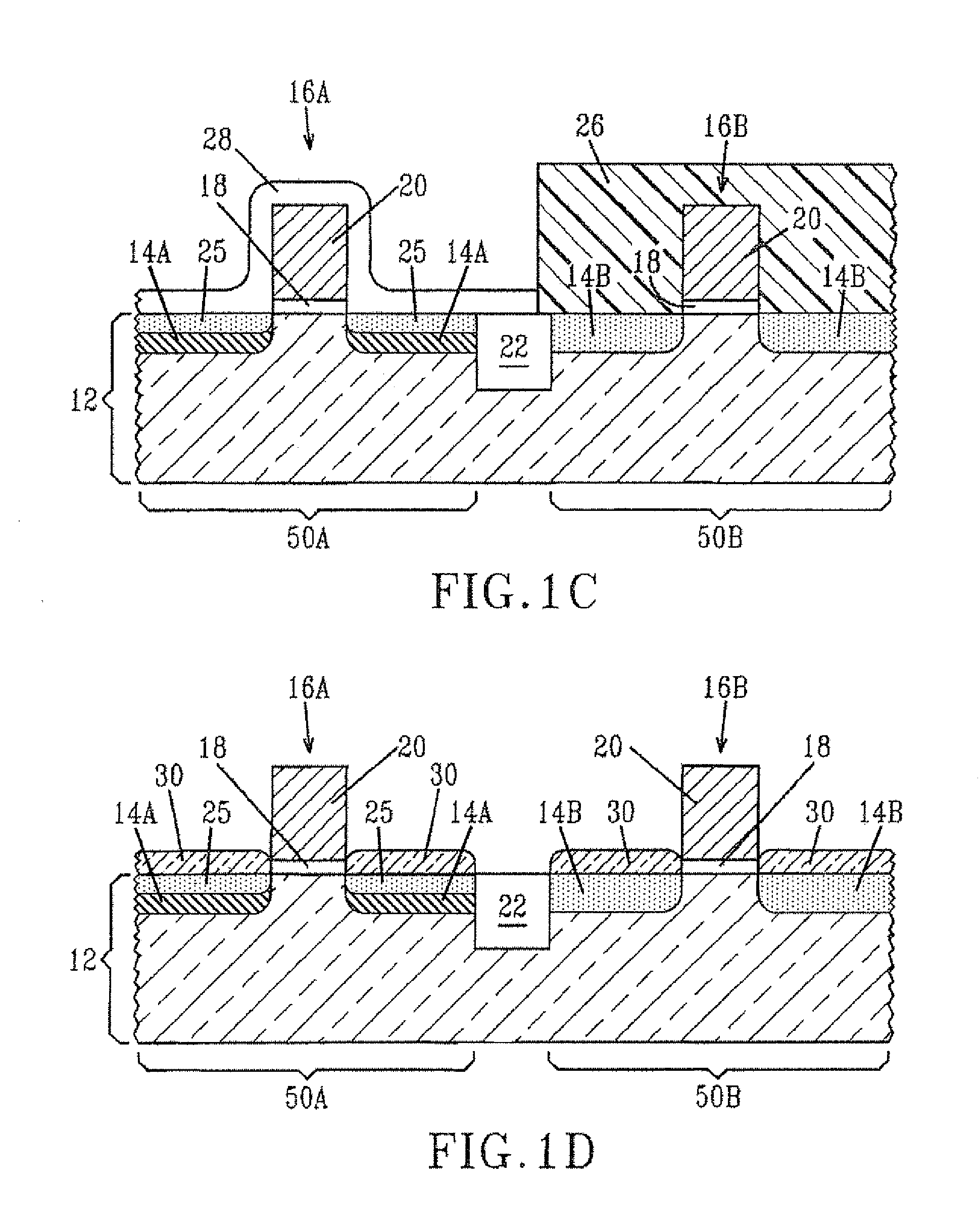
[0006]The present invention describes a method that allows for simultaneous, uniform selective or non-selective epitaxial growth of a material on similar or dissimilar surfaces that does not impart substrate thinning via a novel surface preparation scheme, as well as a structure that results from the implementation of this scheme into the process integration flow for integrated circuitry. The dissimilar surfaces are typically doped surfaces such as, but not limited to: the source / drain region and / or the gate region of a field effect transistor (FET). When dissimilar surfaces are present, the method of the present invention typically provides a way to modify one of the dissimilar surfaces via interfacial doping such that it has substantially the same growth rate of an epitaxial material and response to surface preparation as one of the other dissimilar surfaces that are not subjected to the interfacial doping. When similar surfaces are present, the method of the present invention typically provides a way to induce a difference in one surface region via interfacial doping such that epitaxial growth of a material in that surface region is prevented.
[0008]The counterdoping method involves implantation of one or more implant species using selected energy and dose conditions in the n-FET and / or p-FET region that effectively affords surface characteristics of the doped region similar to that of its counterpart such that any subsequent pre-epitaxy surface preparation can be universal in affording similar surfaces for uniform, simultaneous epitaxial growth, but still allows for appropriate device performance. The energy and dose of the dominant implant species may be adjusted to afford desired performance. The counterdoping conditions are chosen to render only the surface affected to make the dissimilar surfaces similar in their response to surface preparation and therefore are generally of low energy and low dose.

Problems solved by technology

As the surface characteristics are rendered dissimilar by nature of the implants (including, but not limited to: halo implant and / or source / drain extension implant), one of two results is often afforded: either a less aggressive surface preparation is imparted that does not effectively remove undesired films from one region leading to inadequate simultaneous growth in one region; or, a more aggressive surface preparation is used which allows simultaneous growth, but results in excessive thinning of the underlying crystalline or polycrystalline surface from which the epitaxial film is grown.

Method used


Image

  • Method for tuning epitaxial growth by interfacial doping and structure including same
  • Method for tuning epitaxial growth by interfacial doping and structure including same
  • Method for tuning epitaxial growth by interfacial doping and structure including same

Examples


Embodiment Construction

[0021]The present invention, which provides a method of interfacial control for selective or non-selective epitaxial growth for semiconductor structures as well as the structures that result from such a method, will now be described in greater detail by referring to the drawings that accompany the present application. It is noted that the drawings of the present invention are provided for illustrative purposes and as such they are not drawn to scale. It is also noted that the following description and drawings describe the inventive method being implemented in fabricating a CMOS structure including RSD. Although such an embodiment is described and illustrated, the inventive method can be used for fabrication of other semiconductor devices, which include the epitaxial growth of a material layer from at least one material region that is doped or undoped.

[0022]FIG. 1A shows an initial structure 10 that can be used in the present invention. As shown, the initial structure 10 includes a ...


PUM

PropertyMeasurementUnit
dielectric constantaaaaaaaaaa

Abstract

A method that allows for uniform, simultaneous epitaxial growth of a semiconductor material on dissimilarly doped semiconductor surfaces (n-type and p-type) that does not impart substrate thinning via a novel surface preparation scheme, as well as a structure that results from the implementation of this scheme into the process integration flow for integrated circuitry are provided. The method of the present invention can by used for the selective or nonselective epitaxial growth of semiconductor material from the dissimilar surfaces. More specifically, the invention comprises a method for counterdoping of n-FET and / or p-FET regions of silicon circuitry during the halo and / or extension implantation process utilizing a technique by which the surface characteristics of the two regions are made similar with respect to their response to wet or dry surface preparation and which renders the two previously dissimilar surfaces amenable to simultaneous epitaxial growth of raised source / drain structures; but not otherwise affecting the electrical performance of the resulting device.

Description

FIELD OF THE INVENTION [0001]The present invention relates to semiconductor device fabrication, and more particularly to a method that allows for simultaneous, uniform selective or non-selective epitaxial growth of a material from similar or dissimilar surfaces by controlling interfacial doping. The present invention also relates to the semiconductor structure that is obtained using the method of the present invention.BACKGROUND OF THE INVENTION [0002]Selective epitaxial growth is the critical unit process for the formation of semiconductor structures including raised source / drain (RSD) regions used to enable silicon integrated circuit technology, such as complementary metal oxide semiconductor (CMOS) structures on a bulk Si-containing semiconductor or a silicon-on-insulator (SOI) and bipolar devices. As with all selective epitaxial processes, the growth of the RSD is highly dependent on the nature of the surface from which it is grown and, in turn, the pre-epitaxy preparation of th...

Claims


Application Information

Patent Timeline
Patent Type & Authority Patents(United States)
IPC IPC(8): H01L21/44
CPCH01L21/823418H01L21/823814H01L29/0847H01L29/66628H01L29/7834H01L21/2236H01L21/2256H01L21/26513
Inventor BABICH, KATHERINA E.DORIS, BRUCE B.MEDEIROS, DAVID R.SADANA, DEVENDRA K.
Owner GLOBALFOUNDRIES INC
Learn More