Innovated technique to reduce memory interface write mode SSN in FPGA

Inactive Publication Date: 2008-02-12
ALTERA CORP
View PDF2 Cites 9 Cited by
  • Summary
  • Abstract
  • Description
  • Claims
  • Application Information

AI Technical Summary

Benefits of technology

[0006]Systems and methods in accordance with various embodiments of the present invention can reduce the amount of simultaneous switch

Problems solved by technology

Simultaneous switching noise (SSN) is one of the many challenges facing the design and implementation of high speed external interfaces.
If the magnitude of the noise is large enough and/or the duration long enough, the noise can adversely affect the functionality of the programmab

Method used


Image

  • Innovated technique to reduce memory interface write mode SSN in FPGA
  • Innovated technique to reduce memory interface write mode SSN in FPGA
  • Innovated technique to reduce memory interface write mode SSN in FPGA

Examples


Embodiment Construction

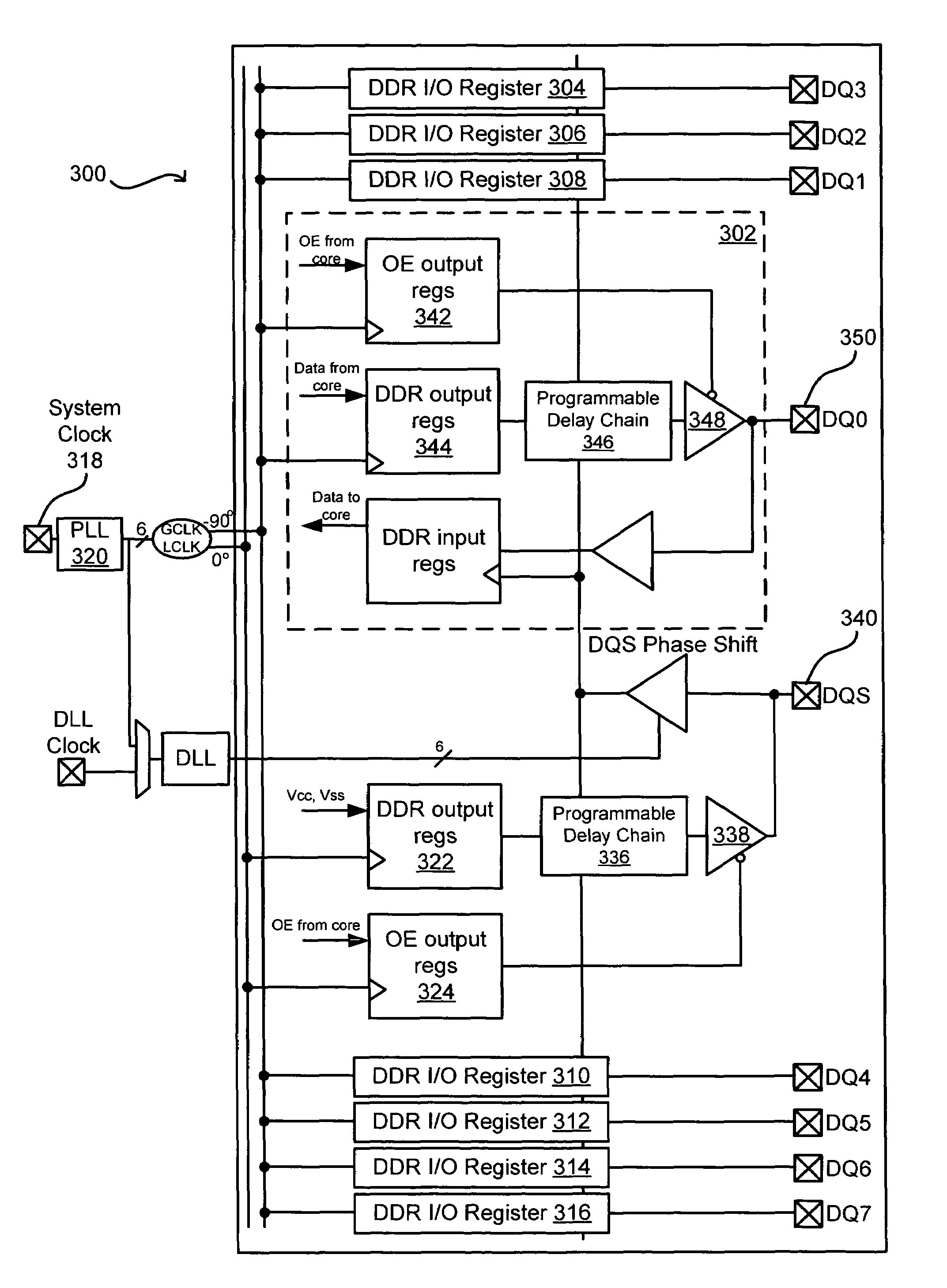
[0020]Systems and methods in accordance with various embodiments of the present invention can overcome these and other deficiencies in existing programmable devices by reducing the amount of noise generated, at least in part, by the simultaneous switching of large numbers of pins. Since simultaneous switching noise can be determined using Δv=L(di / dt), where Δv is the change in voltage, L is the inductance, and di / dt is the change in current over time, the noise can be reduced by controlling variations in current in a programmable device.

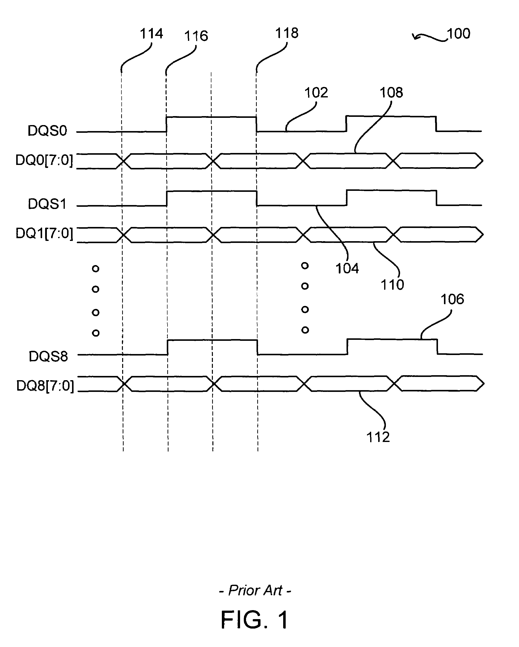
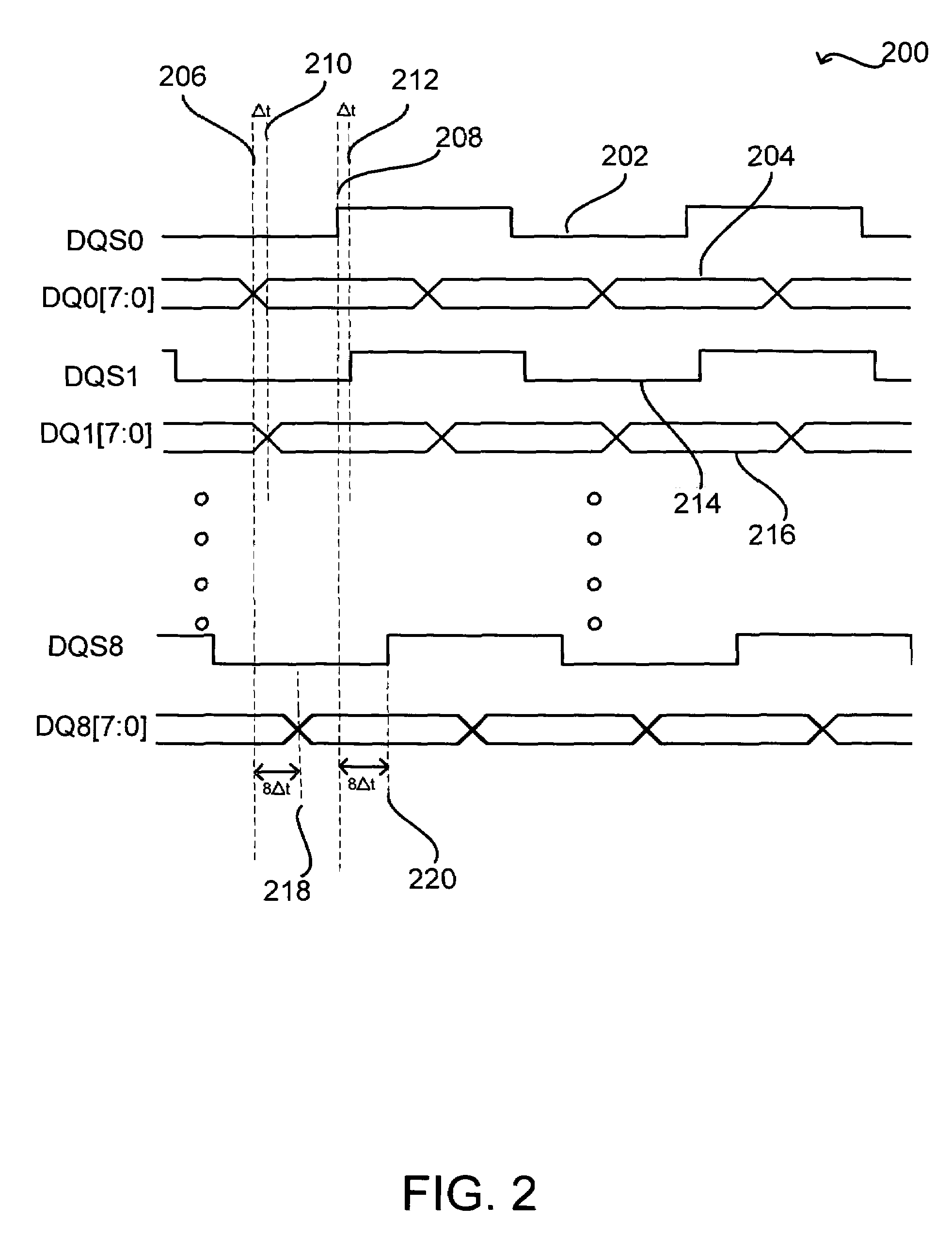
[0021]The relative timing of I / O pins for an example interface implemented in a prior programmable device can be described with respect to the timing diagram 100 of FIG. 1. The I / O pins of a prior I / O bank can be partitioned into a number of subsets, such as nine subsets of I / O pins, each subset outputting a strobe signal (DQ0 through DQ7). For simplicity, only three of these strobe signals (102, 104, 106) are shown, as each DQS signal would appear i...


PUM


Abstract

The amount of simultaneous switching noise generated through the operation of a programmable device can be reduced by reducing the number of pins switching at the same time. An I/O bank can include a number of I/O pin subsets, or DQS groups, each programmed to switch at a different time so that the switching times of the various pins can be staggered for each system clock cycle. Programmable delay elements can be used to control the delay of each subset. The programmable elements can be placed between the system clock and the output registers in order to delay the receiving of the clock signal by the registers and therefore delaying the switching of the output buffers. The programmable delay elements also can be placed between the output registers and the output buffers in order to delay the receiving of the output data by, and subsequent switching of, the output buffers.

Description

BACKGROUND[0001]The present invention relates to the field of programmable devices, and systems and methods for programming the same. Programmable devices, such as field programmable gate arrays (FPGAs), typically include thousands of programmable logic cells that use combinations of logic gates and / or look-up tables to perform logic operations. Programmable devices typically also include a number of functional blocks having specialized logic devices adapted to specific logic operations, such as adders, multiply and accumulate circuits, phase-locked loops, and one or more embedded memory array blocks. The logic cells and functional blocks typically are interconnected with a configurable switching circuit, which selectively routes connections between the logic cells and functional blocks. By configuring the combination of logic cells, functional blocks, and the switching circuit, a programmable device can be adapted to perform virtually any type of information processing function.[00...

Claims


Application Information

Patent Timeline
IPC IPC(8): H03K19/173
CPCH03K19/17744
Inventor HUANG, JOSEPHSUNG, CHIAKANGCHU, MICHAEL H. M.CHONG, YAN
Owner ALTERA CORP
Why Eureka
Try Eureka