Electronic circuit, display device, and electronic apparatus

Inactive Publication Date: 2008-02-19
SEMICON ENERGY LAB CO LTD
View PDF29 Cites 2 Cited by
  • Summary
  • Abstract
  • Description
  • Claims
  • Application Information

AI Technical Summary

Benefits of technology

[0016]Generally, the variation in the electrical characteristic of a polysilicon TFT is generated easily due to defects and the like in a crystal grain boundary. In the circuit of FIG. 3, by arranging the transistors 312 and 313 adjacently, the variation

Problems solved by technology

That is, a module is large and complicated in a conventional PM type (passive matrix type) and an AM type which is using

Method used


Image

  • Electronic circuit, display device, and electronic apparatus
  • Electronic circuit, display device, and electronic apparatus
  • Electronic circuit, display device, and electronic apparatus

Examples


embodiment mode 1

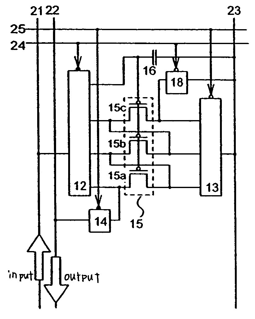
[0032]An outline of a current data compression circuit of the invention is now explained with reference to FIGS. 1 and 2.

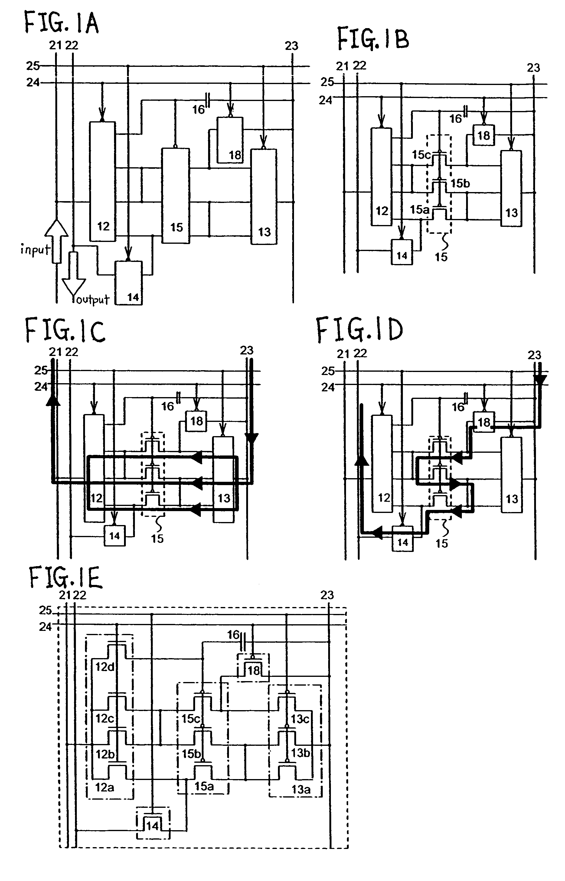
[0033]First, FIG. 1 is explained. FIG. 1A shows an example of the current data compression circuit of the invention. FIG. 1B shows FIG. 1A in which a drive element is illustrated by three transistors.

[0034]The current data compression circuit of FIGS. 1A and 1B include a first switch 12, a second switch 13, a third switch 14, and a fourth switch 18 besides a drive element 15. As for each of first to fourth switches in FIG. 1, a point of ∘ (open circle) or ● (close circle) denotes a control portion of the switches, and each of other plurality of points becomes conductive or open simultaneously in accordance with the signal sent to the control portion. The control portion ∘ (open circle) denotes low active (conductive when signal is low), and the control portion ● (close circle) denotes high active (conductive when signal is high). The first switch 12, the second sw...

embodiment mode 2

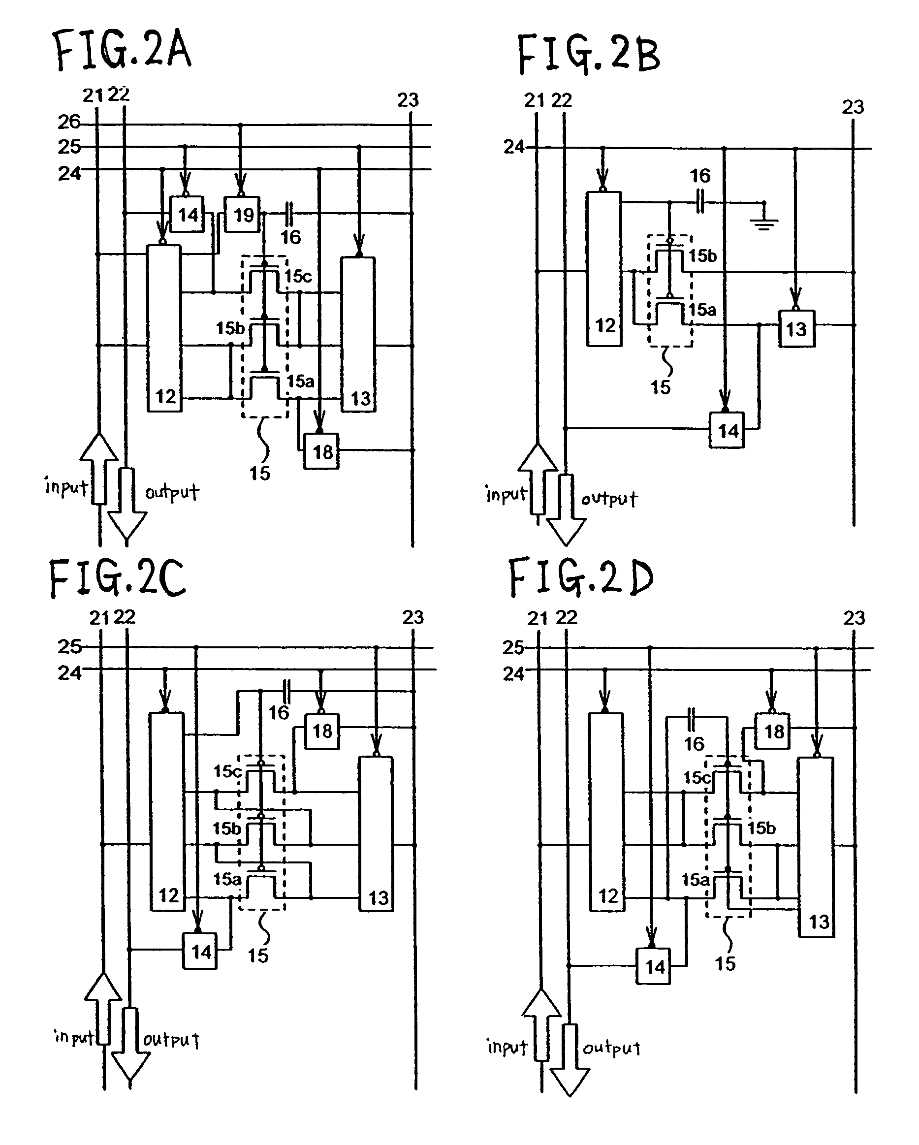
[0041]FIG. 2 is explained now. FIGS. 2A to 2D show four other examples of a current data compression circuit of the invention. It should be noted that a current data compression circuit of the invention can be configured in so many various ways that all of them cannot be shown, thus FIGS. 2A to 2D are only representative examples.

[0042]Each of first to fourth switches of FIG. 2 is the same as the ones in FIG. 1. ∘ (open circle) or ● (close circle) is a control portion of the switches, and each of other plurality of points becomes conductive or open simultaneously in accordance with the signal sent to the control portion. The control portion ∘ (open circle) denotes low active (conductive when signal is low), and the control portion ● (close circle) denotes high active (conductive when signal is high). Each of the switches in FIG. 2 can be illustrated by transistors as is in FIG. 1E, however, it is omitted here for simplicity.

[0043]FIG. 2A shows a configuration example in which a driv...

embodiment mode 3

[0077]An example of a data driver circuit of an AM type OLED display device, to which the current data compression circuit of the invention is applied is explained with reference to FIGS. 7 to 9 in Embodiment Mode 3. The data driver circuit in this example is such type of circuit that a video signal of an original analog current value is read in and a video signal of a compressed analog current is written to a data line.

[0078]FIG. 8 shows an outline of the AM type OLED display device. Each data line 810 and each scan line 820 are disposed in a matrix in a pixel portion 831. A scan driver circuit 821 outputs a selection pulse to each scan line 820 in sequence. Each data line 810 transmits a video signal, which is outputted from a data driver circuit 811 in synchronous with the selection pulse, to the pixel portion 831.

[0079]A portion surrounded by a broken line 812 corresponds to a unit of data driver circuit configured as 740 in FIG. 7 by which the video signal is written to each da...


PUM


Abstract

A current data compression circuit of which output current value is accurate even when transistors with large variations in electrical characteristics are used. The current data compression circuit is an electronic circuit comprising a drive element including a plurality of transistors and a means for switching over a series connection state and a parallel connection state of the transistors. An inputted current is compressed for output by the current data compression circuit. Or, the current data compression circuit is an electronic circuit comprising a drive element including a plurality of transistors in which the transistors are used in parallel connection states when inputting current and in series connection states when outputting current.

Description

BACKGROUND OF THE INVENTION[0001]1. Field of the Invention[0002]The present invention relates to an electronic circuit and more particularly a technology of an electronic circuit which compresses current data. Also the invention relates to an integrated circuit (IC) or a system circuit using the electronic circuit in one portion thereof, and more particularly a display device or an electronic apparatus having the IC or the system circuit.[0003]2. Description of the Related Art[0004]As electronic apparatus has been advanced in high performance, compactness (miniaturization) and low power consumption, an IC (integrated circuit) used inside thereof is required to be high in performance, small and highly integrated and such demands are further growing. A MOSFET (Field-Effect Transistor) IC using a conventional general bulk silicon (silicon wafer) has been progressed in performance, compactness and integration steadily up to now and this tendency is likely to continue.[0005]An IC using a...

Claims


Application Information

Patent Timeline
IPC IPC(8): G06F3/038G09G5/00G09G3/10G09G3/30
CPCG09G3/30G09G2310/0275
Inventor INUKAI, KAZUTAKA
Owner SEMICON ENERGY LAB CO LTD
Why Eureka
Try Eureka