Laser annealing apparatus

a technology of laser annealing and annealing chamber, which is applied in the direction of chemically reactive gas growth, crystal growth process, polycrystalline material growth, etc., can solve the uneven laser energy supplied to silicon substrate, uneven surface of silicon substrate, etc., to achieve the effect of minimizing dislocation

Inactive Publication Date: 2008-02-26
LG DISPLAY CO LTD
View PDF8 Cites 2 Cited by
  • Summary
  • Abstract
  • Description
  • Claims
  • Application Information

AI Technical Summary

Benefits of technology

[0017]The invention, in part, provides a laser annealing apparatus capable of performing uniform laser crystallization on an entire silicon substrate by minimizing the dislocation of the silicon substrate during laser beam irradiation. The minimized dislocation can be achieved by installing a vacuum chuck holding the silicon substrate in a movable stage.
[0018]The invention, in part, provides a laser annealing apparatus which can carry out uniform laser crystallization on an entire silicon substrate by minimizing the unevenness of the silicon substrate. The minimized unevenness can be achieved by using a vacuum chuck that holds the silicon substrate using a vacuum attachment.

Problems solved by technology

A further complicating factor is the uneveness of the surface of the silicon substrate.
The focal point of the laser is fixed, but the surface of the silicon substrate is uneven.
The variation of the distance between the silicon substrate and the focus of the laser beam results in unevenness of laser energy with which the silicon substrate is supplied.
The resulting laser crystallization, which should be carried out with continuous and uniform conditions, produces a poor result.
Thus, discontinuation of crystallization may result instead of continuous growth of the silicon grain.
As has been shown, the conventional SLS technology is hampered by discontinuities which inhibit the continuous growth of silicon grains.

Method used


Image

  • Laser annealing apparatus
  • Laser annealing apparatus
  • Laser annealing apparatus

Examples


Embodiment Construction

[0026]Advantages of the present invention will become more apparent from the detailed description given herein after. However, it should be understood that the detailed description and specific examples, while indicating preferred embodiments of the invention, are given by way of illustration only, since various changes and modifications within the spirit and scope of the invention will become apparent to those skilled in the art from this detailed description.

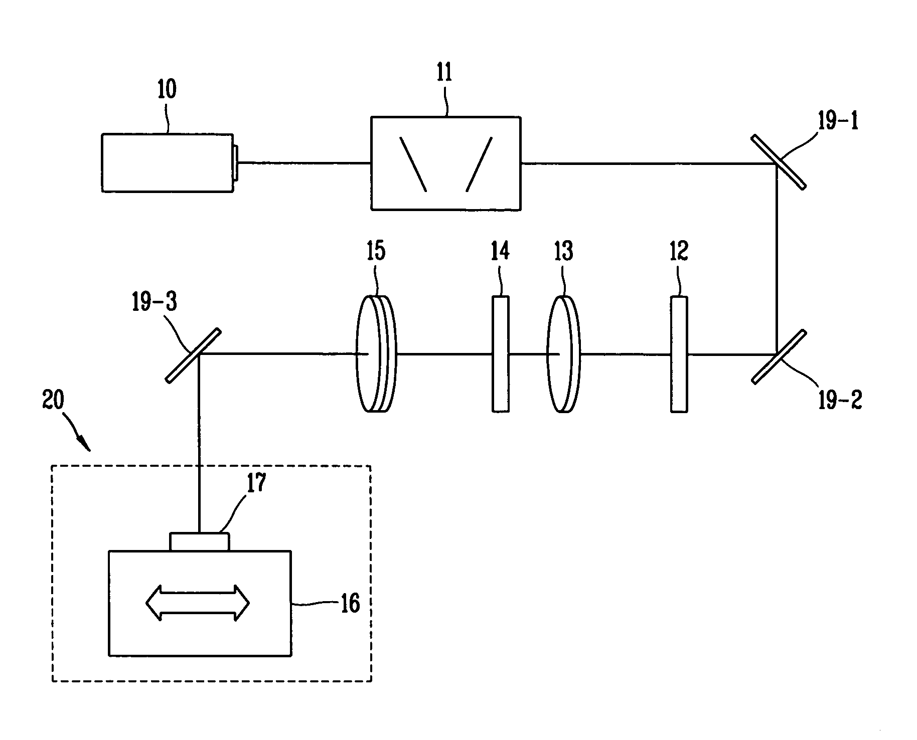
[0027]FIG. 1 shows a laser annealing apparatus for use in sequential lateral solidification (SLS).

[0028]When crystallizing a silicon film by SLS, a laser beam is patterned to a predetermined shape, and the silicon film is continusously irradiated with the patterned laser beam.

[0029]For crystallizing the silicon film, an unpatterned initial laser beam irradiates from a laser source 10 and passes through an attenuator 11, a homogenizer 12, and a field lens 13, thereby both controlling the energy of and condensing the laser beam....


PUM

PropertyMeasurementUnit
widthaaaaaaaaaa
energyaaaaaaaaaa
lengthaaaaaaaaaa

Abstract

A laser annealing apparatus for sequential lateral solidification (SLS) to uniformly crystallize silicon on an entire silicon substrate by minimizing the dislocation of the silicon substrate during laser beam irradiation is disclosed.During the laser annealing, a vacuum chuck holds the silicon substrate on a movable stage. The device includes a laser source, an optical system patterning the shape and energy of a laser beam irradiated from the laser source, a vacuum chuck supporting a silicon substrate, and a movable stage supporting the vacuum chuck as well as transferring the vacuum chuck in a predetermined direction. Accordingly, the apparatus improves the degree of crystallization because it is able to uniformly carry out SLS on an entire surface of the silicon substrate.

Description

[0001]This application is a continuation-in-part application of application Ser. No. 10 / 211,570, filed on Aug. 5, 2002 now U.S. Pat. No. 6,852,162, and for which priority is claimed under 35 U.S.C. § 120; application Ser. No. 10 / 211,570 is a divisional application of application Ser. No. 09 / 697,510, filed Oct. 27, 2000, now U.S. Pat. No. 6,514,339; and priority is claimed under 35 U.S.C. § 119 to application Ser. No. 99-47532 filed in Korea on Oct. 29, 1999. Each of the above-described applications are hereby incorporated by reference in their entirety.FIELD OF INVENTION[0002]A laser annealing apparatus is used for sequential lateral solidification (SLS) to crystallize silicon.DISCUSSION OF RELATED ART[0003]Sequential laser solidification (SLS) is used for crystallizing a silicon film by using the fact that silicon grains grow perpendicularly to an interface between a liquid silicon region and a solid silicon region, i.e., into the molten silicon or melt zone. SLS differs from a con...

Claims


Application Information

Patent Timeline
Patent Type & Authority Patents(United States)
IPC IPC(8): C30B35/00C30B13/00C30B13/24
CPCC30B13/24C30B29/06Y10T117/10Y10S117/90
Inventor JUNG, YUN-HO
Owner LG DISPLAY CO LTD
Why Eureka
Try Eureka