Semiconductor substrate

a technology of semiconductor substrate and substrate, which is applied in the manufacture of semiconductor/solid-state devices, semiconductor devices, electrical apparatus, etc., can solve the problems of cracks, reduced crystallinity, and forming of various defects in the compound semiconductor layer, so as to improve crystallinity, improve the crystallinity, and maximize the compressive strain

Active Publication Date: 2017-02-28
LG SILTRON
View PDF29 Cites 0 Cited by
  • Summary
  • Abstract
  • Description
  • Claims
  • Application Information

AI Technical Summary

Benefits of technology

[0016]According to an embodiment, compressive strain may be maximized by including a buffer layer including a plurality of step regions having different amounts of aluminum (Al) and reducing the amount of Al in the step region of the lowermost region of the buffer layer in contact with a seed layer by at least 30% in comparison to an amount of Al in the seed layer, and thus, a thick, crack-free conductive type semiconductor layer may be grown.
[0017]According to an embodiment, a heterogeneous region is formed between the plurality of step regions of the buffer layer to make the top surface of a semiconductor layer above the heterogeneous region as a flat surface, and thus, crystallinity may be improved.
[0018]According to an embodiment, the heterogeneous region blocks dislocations generated in the buffer layer, and as a result, the generation of dislocations in a nitride semiconductor layer formed on the heterogeneous region may be minimized to improve the crystallinity.
[0019]According to an embodiment, stress is controlled by the heterogeneous region and the step regions by disposing the heterogeneous region between the step regions of the buffer layer, and thus, cracks may not only occur in a nitride layer formed on the buffer layer, but a growth substrate may also not be broken.
[0020]According to an embodiment, dislocations of the buffer layer are primarily blocked by mask patterns of a mask layer and dislocations moving in a vertical direction between the mask patterns are guided to a horizontal direction, thereby enabling the dislocations not to move in the vertical direction any more. Accordingly, since dislocations may hardly occur in a nitride semiconductor formed on the mask layer, a decrease in the crystallinity due to the dislocations may be prevented.
[0021]According to an embodiment, since a crystallinity control layer including a plurality of mask layers and a plurality of nitride semiconductor layers is formed to increase compressive strain, tensile strain generated during cooling in post processing is compensated. Thus, cracks may not only occur in a nitride semiconductor layer formed on the crystallinity control layer, but a growth substrate may also not be broken.BRIEF DESCRIPTION OF THE FIGURES

Problems solved by technology

In the semiconductor substrate, various defects may be formed due to a difference in lattice constants, thermal expansion coefficients, or strains between the growth substrate and the compound semiconductor layer.
A typical semiconductor substrate has limitations in that crystallinity may be decreased by the generation of dislocations caused by the difference in the lattice constants between the growth substrate and the compound semiconductor layer.
In addition, the differences in the lattice constants and the thermal expansion coefficients between the growth substrate and the compound semiconductor layer cause strain.
That is, a balance between compressive strain during the growth of compound semiconductors and tensile strain during cooling to room temperature after the growth does not match, and eventually, cracks may occur in the compound semiconductor layer or the growth substrate may be broken.
With respect to a typical semiconductor substrate, since cracks may occur in the compound semiconductor layer, a high-quality, thick semiconductor layer substantially functioning as an electronic device may not be grown.

Method used


Image

  • Semiconductor substrate
  • Semiconductor substrate
  • Semiconductor substrate

Examples


first embodiment

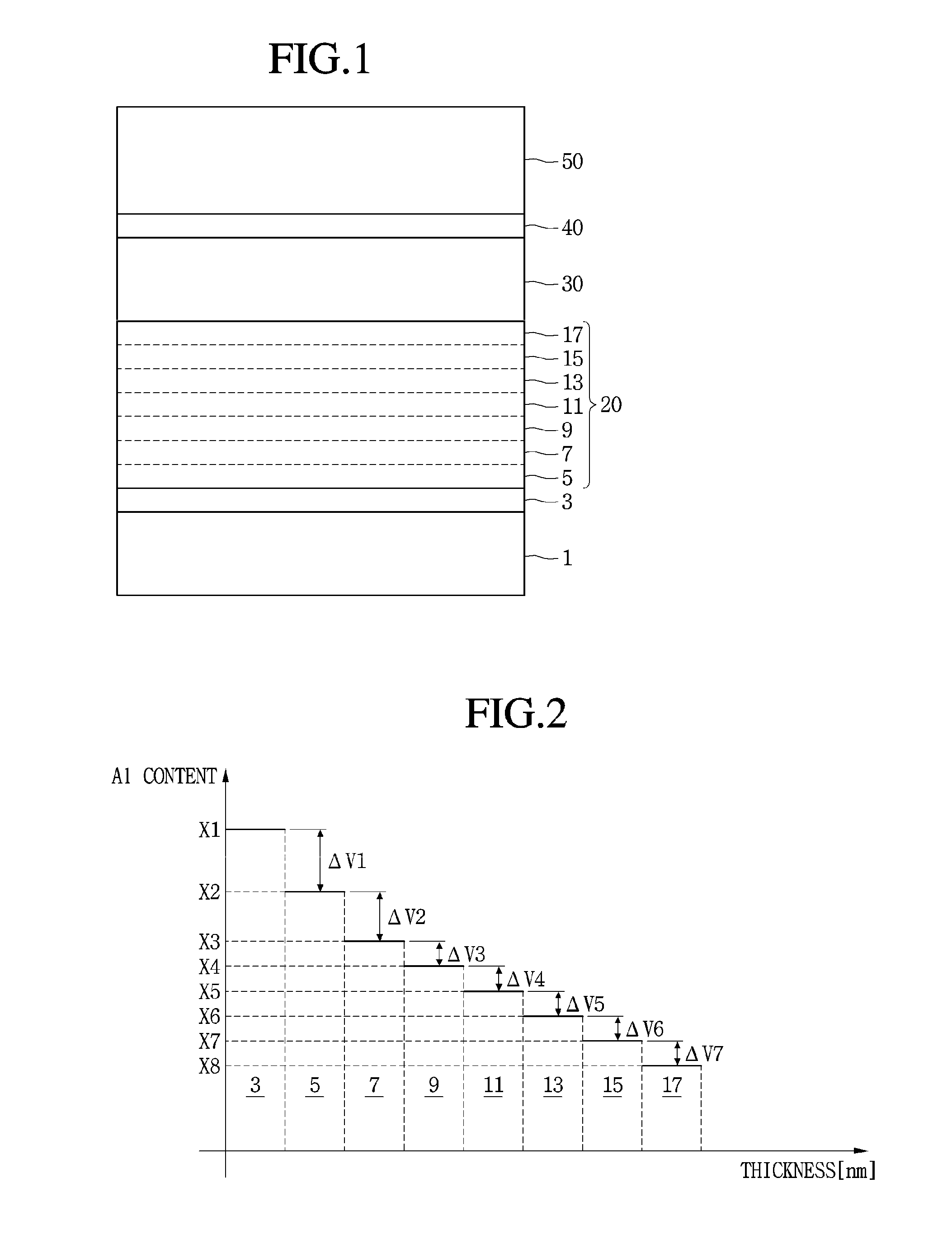
[0044]FIG. 1 is a cross-sectional view illustrating a semiconductor substrate according to a

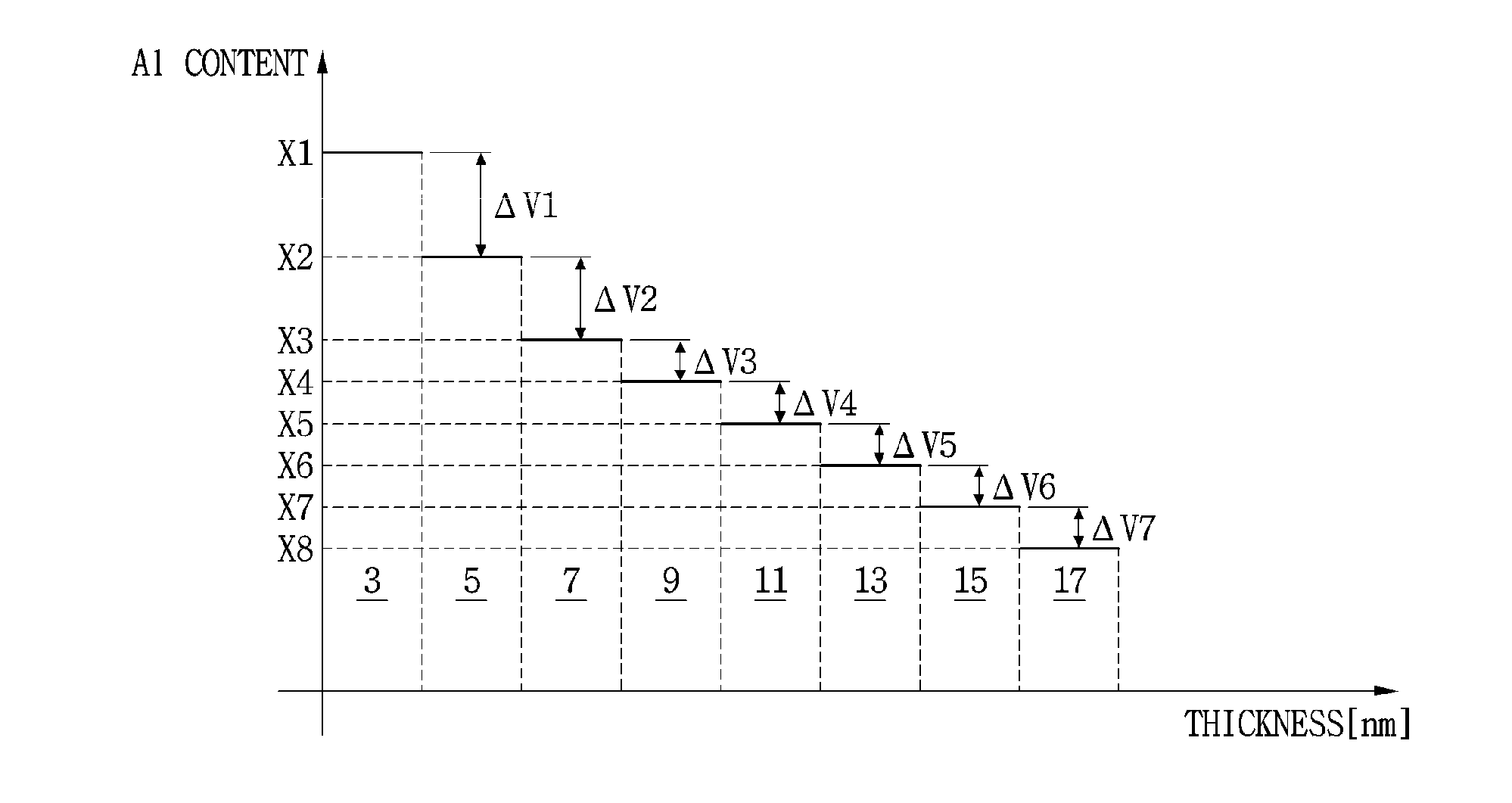
[0045]Referring to FIG. 1, the semiconductor substrate according to the first embodiment may include a growth substrate 1, a seed layer 3, a buffer layer 20, a first nitride semiconductor layer 30, a stress control layer 40, and a second nitride semiconductor layer 50.

[0046]The at least one stress control layer 40 may be formed, but the present disclosure is not limited thereto.

[0047]The semiconductor substrate according to the first embodiment may function as a base substrate for preparing an electronic device, such as a solar cell, a photodetector, or a light-emitting device, but the present disclosure is not limited thereto.

[0048]The seed layer 3, the buffer layer 20, the first nitride semiconductor layer 30, the stress control layer 40, and the second nitride semiconductor layer 50 may be formed of Group II-IV and / or Group III-V compound semiconductor materials, but the present disclosure...

second embodiment

[0115]FIG. 9 is a cross-sectional view illustrating a semiconductor substrate according to a

[0116]The second embodiment is substantially similar to the first embodiment except a buffer layer 20 including a plurality of step regions 5, 7, 9, 11, 13, 15, and 17 and a single heterogeneous region 62. Thus, in the following description of the second embodiment, the same reference numerals will be assigned to the same elements having the same shape or function as those of the first embodiment and the details thereof will be omitted.

[0117]Referring to FIG. 9, the semiconductor substrate according to the second embodiment may include a growth substrate 1, a seed layer 3, the buffer layer 20, a first nitride semiconductor layer 30, a stress control layer 40, and a second nitride semiconductor layer 50.

[0118]The buffer layer 20 may include first to seventh step regions 5, 7, 9, 11, 13, 15, and 17 and the heterogeneous region 62. The heterogeneous region 62 may be formed between any one of the...

third embodiment

[0135]FIG. 12 is a cross-sectional view illustrating a semiconductor substrate according to a

[0136]The third embodiment is a modification of the second embodiment in which a plurality of heterogeneous regions 62a, 62b, 62c, 62d, 62e, and 62f is disposed between first to seventh step regions 5, 7, 9, 11, 13, 15, and 17. The description below will be briefly given, and any details not described herein will be easily understood from the first and second embodiments.

[0137]Referring to FIG. 12, the semiconductor substrate according to the third embodiment may include a growth substrate 1, a seed layer 3, a buffer layer 20, a first nitride semiconductor layer 30, a stress control layer 40, and a second nitride semiconductor layer 50.

[0138]The buffer layer 20 may include the first to seventh step regions 5, 7, 9, 11, 13, 15, and 17 and the first to sixth heterogeneous regions 62a, 62b, 62c, 62d, 62e, and 62f formed between the first to seventh step regions 5, 7, 9, 11, 13, 15, and 17.

[0139...


PUM


Abstract

Provided is a semiconductor substrate including a seed layer disposed on a substrate, a buffer layer disposed on the seed layer, a plurality of nitride semiconductor layers disposed on the buffer layer, and at least one stress control layer between the plurality of nitride semiconductor layers. The buffer layer includes a plurality of step regions and at least one heterogeneous region. The plurality of step regions includes the same nitride semiconductor material. The heterogeneous region includes a different nitride semiconductor material from the step regions.

Description

CROSS-REFERENCE TO RELATED APPLICATIONS[0001]The present application is a national phase application of International Application PCT / KR2014 / 000021, with an international filing date of Jan. 3, 2014, which claims the priority benefit of Korean Application No. 10-2013-0003983, filed Jan. 14, 2013, the contents of which are incorporated herein by reference in their entirety for all purposes.BACKGROUND OF THE INVENTION[0002]1. Field of the Invention[0003]The present disclosure relates to a semiconductor substrate.[0004]2. Description of the Related Art[0005]Various electronic devices using compound semiconductor materials have been developed.[0006]Solar cells, photodetectors, and light-emitting devices may be used as electronic devices.[0007]Such electronic devices may be fabricated on the basis of a semiconductor substrate. The semiconductor substrate includes a growth substrate and a compound semiconductor layer grown thereon.[0008]In the semiconductor substrate, various defects may ...

Claims


Application Information

Patent Timeline
Patent Type & Authority Patents(United States)
IPC IPC(8): H01L29/15H01L29/66H01L31/06H01L29/205H01L29/20H01L21/02
CPCH01L29/205H01L21/0254H01L21/02458H01L21/02507H01L29/2003H01L21/20H01L29/36
Inventor LEE, KYE-JINLEE, HO-JUNCHOI, YOUNG-JAEEUM, JUNG-HYUNLEE, CHUNG-HYUN
Owner LG SILTRON
Why Eureka
Try Eureka