EMI shielded integrated circuit packages and methods of making the same

a shielded integrated circuit and shielded technology, applied in the field of shielded integrated circuit packages and methods of making the same, can solve the problems of electromagnetic interference (emi) to signal integrity, interfere with the thermal profile necessary to achieve well-formed and reliable solder joints, and the inspection of solder joints becomes impossible, so as to reduce the area and volume, and minimize the dislocation of electromagnetic fields. , the effect of simplifying the full cleaning and inspection of both sides

Active Publication Date: 2019-06-11
LEXIWAVE TECH HONG KONG +1
View PDF8 Cites 0 Cited by
  • Summary
  • Abstract
  • Description
  • Claims
  • Application Information

AI Technical Summary

Benefits of technology

[0015]Embodiments of the present invention include the use of a pre-assembled circuit module and interposer to provide a plurality of EMI shielded structures for components mounted on the underside or both sides of a circuit module substrate within a single package and methods to form such semiconductor packages, thereby substantially reducing both area and volume necessary for the construction of shielded assemblies.
[0016]In one embodiment, a semiconductor package includes a Faraday Cage formed when a pre-tested circuit module with components mounted thereon and incorporating a suitable ground or reference plane is affixed to an interposer structure containing cavities which provide clearance for the components on the underside of the circuit module. The walls and floor of said cavities are coated with a suitable conductive composition, e.g. plated copper, and ridges between the cavities and contact pads or conduction paths around the perimeter of the mounting surface on which the circuit module is placed make contact with corresponding contact pads or conduction paths on the circuit module, thereby creating an equipotential between the cavity walls and floor and the ground or reference plane in the circuit module and creating a closed Faraday Cage. An alternative embodiment provides lateral shielding using rows of vias or conductive posts formed around the cavity within the interposer and electrically connected to both the circuit module reference plane and the shield plane on the floor of the cavity, said vias or posts having a spacing appropriate to the formation of the Faraday Cage. In a further embodiment, the rows of vias within the interposer are matched by rows of vias in the circuit module which connect contact pads or conduction paths or strips on the carrier surface to the carrier ground or reference plane. The carrier vias are placed such that they are coaxial with the vias in the interposer, thereby minimizing dislocations within the electromagnetic field formed by the via array. As the circuit module can be assembled and functionally tested before being mounted into the interposer, the present invention further enables simplified full cleaning and inspection of both sides of the assembled module as well as functional testing and eliminates the need for a shield can on at least one side of the circuit module. In a further embodiment the present invention can also provide an environmental or hermetic, sealed environment for circuit elements on at least one side of the circuit module.

Problems solved by technology

Increasingly miniaturized system-in-package (SiP) devices used in a growing number of static and mobile devices present problems of electromagnetic interference (EMI) to signal integrity while at the same time some of the components can radiate electromagnetic energy which can interfere with other circuit elements.
For example, a SiP device packaging a digital processor chip generates electromagnetic energy which can interfere with the operation of a high sensitivity low noise radio frequency amplifier in the same SiP.
Since the shield cans are covering the components during the solder reflow process, this may interfere with the thermal profile necessary to achieve well-formed and reliable solder joints.
With the shield can soldered in place, inspection of solder joints becomes impossible, and rework becomes more complex and problematic should that be required.
As a result, shield cans are available with snap-on lids, but this often adds size and complexity to the shield enclosure and may compromise the shielding effectiveness of the can.
In compact, high density designs, and in particular modular assemblies operating at RF equivalent frequencies packaged as components for assembly onto a motherboard, preformed metal cans become less attractive.
This makes the use of multiple, single cavity shield cans impractical when several cavities are needed.
Another limitation of this approach derives from the assembly process.
Since the shield cans are mounted and fixed by reflow of solder paste, it becomes impractical to mount them on both sides of a circuit module substrate or a circuit board, as the shield cans mounted in the first pass would fall off in the second pass unless glued in place.
Gluing the cans in the first pass would eliminate any possibility for rework or inspection unless removable lid types were used, adding complexity, cost, and degrading the shielding capabilities of the enclosure.
Yet another limitation is found in the use of shield cans in that cleaning of flux residues and other byproducts of the reflow operation becomes problematic if not impossible under the shield can.
Yet at the same time the shield can cannot provide a hermetic enclosure due to the need for either holes or a removable lid during the reflow process as discussed above.
As a consequence, this approach is often impossible, not feasible, and / or too expensive to use in the construction of a high density device.

Method used


Image

  • EMI shielded integrated circuit packages and methods of making the same
  • EMI shielded integrated circuit packages and methods of making the same
  • EMI shielded integrated circuit packages and methods of making the same

Examples


Embodiment Construction

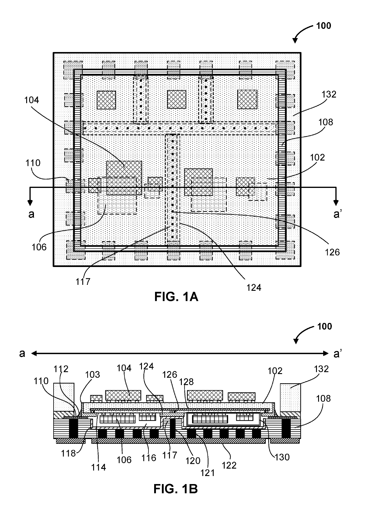
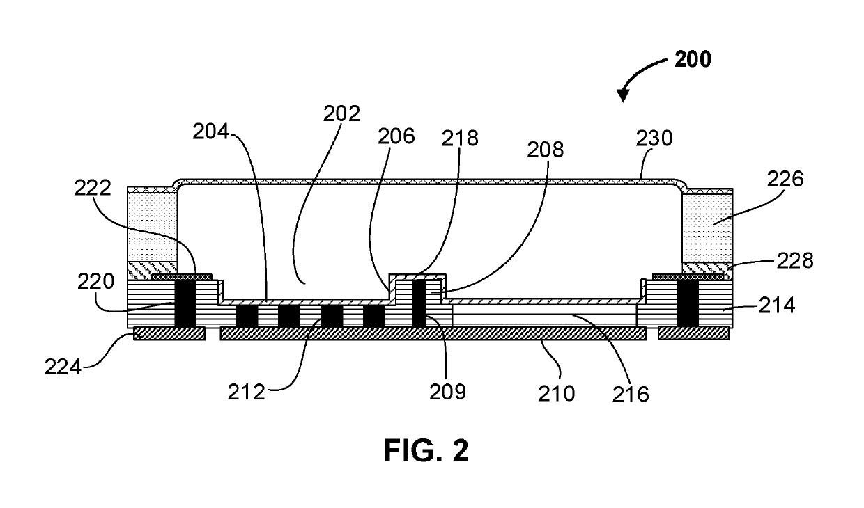
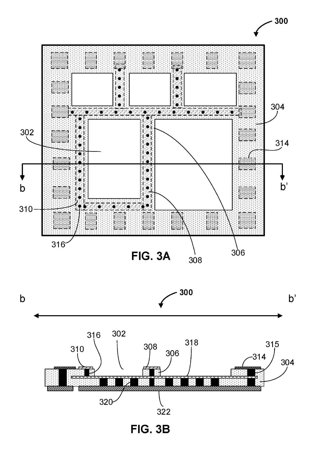
[0024]EMI shielded integrated circuit interposer packages with interposer and circuit module assemblies and methods to form such semiconductor packages are described. In the following description, numerous specific details are set forth, such as packaging architectures and material regimes, in order to provide a thorough understanding of embodiments of the present invention. It will be apparent to one skilled in the art that embodiments of the present invention may be practiced without these specific details. In other instances, well-known features, such as via structure and integrated circuit design layouts, are not described in detail in order to not unnecessarily obscure embodiments of the present invention. Furthermore, it is to be understood that the various embodiments shown in the Figures are illustrative representations and are not necessarily drawn to scale.

[0025]Although interposer packages are known and have been used for many years, their function has generally been limi...


PUM


Abstract

An integrated circuit package with a plurality of embedded electromagnetic interference (EMI) shielding and methods of making the same are disclosed. The integrated circuit packages include the use of a pre-assembled circuit module and an interposer. The circuit module has a plurality of spaced electrical component sections separated by a series of contiguous conductive spacers, and a first shielding means comprises the spacers, vias and an embedded conductive plane. In an example, the interposer has a second shielding means comprises conductive cavities, conductive ridges, vias, and a conduction pattern. In another example, the interposer further comprises conductive strips to form the second shielding means. The first shielding means overlaps the second shielding means to form a plurality of EMI shielded enclosures for holding the spaced electrical component sections therein.

Description

CROSS-REFERENCE TO RELATED APPLICATIONS[0001]This application is the National Stage entry of PCT / US2017 / 018016, filed on Feb. 15, 2017, which claims priority to U.S. Provisional Application No. 62 / 295,480, filed on Feb. 15, 2016, which are incorporated herein by reference in their entireties.FEDERALLY SPONSORED RESEARCH[0002]None.SEQUENCE LISTING[0003]None.CLAIM OF PRIORITY[0004]This application claims priority to U.S. Provisional Patent Application No. 62 / 295,480 filed on Feb. 15, 2016 titled “Method of Faraday Cage Formed within an Integrated Circuit Package with Interposer and Chip Carrier and EMI Shielded Integrated Circuit Interposer Packages Produced and Used in Electronic Assemblies Using This Method” which is incorporated by reference in its entirety.TECHNICAL FIELD[0005]Embodiments of the invention are in the field of semiconductor packages and, in particular, Faraday Cages formed and embedded within integrated circuit interposer and circuit module assemblies.BACKGROUND[000...

Claims


Application Information

Patent Timeline
Patent Type & Authority Patents(United States)
IPC IPC(8): H01L23/552H01L25/16H01L23/538H01L23/498H01L21/56H05K1/14H01L21/48
CPCH01L23/552H01L21/4857H01L21/56H01L23/5385H01L25/165H05K1/144H01L23/49827H01L2224/16225
Inventor WONG, CHIH WEILAU, HENRY
Owner LEXIWAVE TECH HONG KONG
Why Eureka
Try Eureka