Nonvolatile semiconductor storage apparatus and method of driving the same

a storage apparatus and non-volatile technology, applied in static storage, digital storage, instruments, etc., can solve the problems of reducing the reducing the use efficiency of memory cell arrays, and increasing the chip area, so as to improve storage efficiency and reduce chip area.

Inactive Publication Date: 2008-03-04
PANASONIC CORP
View PDF6 Cites 72 Cited by
  • Summary
  • Abstract
  • Description
  • Claims
  • Application Information

AI Technical Summary

Benefits of technology

[0024]According to the structure, an address which can be read in a short time in multivalued information stored in one memory cell is set to be a high speed reading region and is distinguished from regions having the other reading speeds. Consequently, it is possible to efficiently write and read information of 2 bits or more in one memory cell array without reducing a using efficiency of the memory cell array.
[0038]In the case in which a plurality of regions is provided for each erasing unit or each word line, furthermore, a part of memory cells in a corresponding region in the memory cell array is used as the region information storage region. Consequently, it is possible to enhance a storage efficiency in the region information storage region and to reduce a chip area.

Problems solved by technology

For this reason, a reading speed is limited, and there is a problem in the case in which a program code requiring a high speed reading operation and various data requiring an increase in a capacity are stored in one memory cell array, for example.
Consequently, a using efficiency of a memory cell array is reduced so that an increase in a chip area cannot be avoided.

Method used


Image

  • Nonvolatile semiconductor storage apparatus and method of driving the same
  • Nonvolatile semiconductor storage apparatus and method of driving the same
  • Nonvolatile semiconductor storage apparatus and method of driving the same

Examples


second embodiment

[0084]A second embodiment according to the invention will be described.

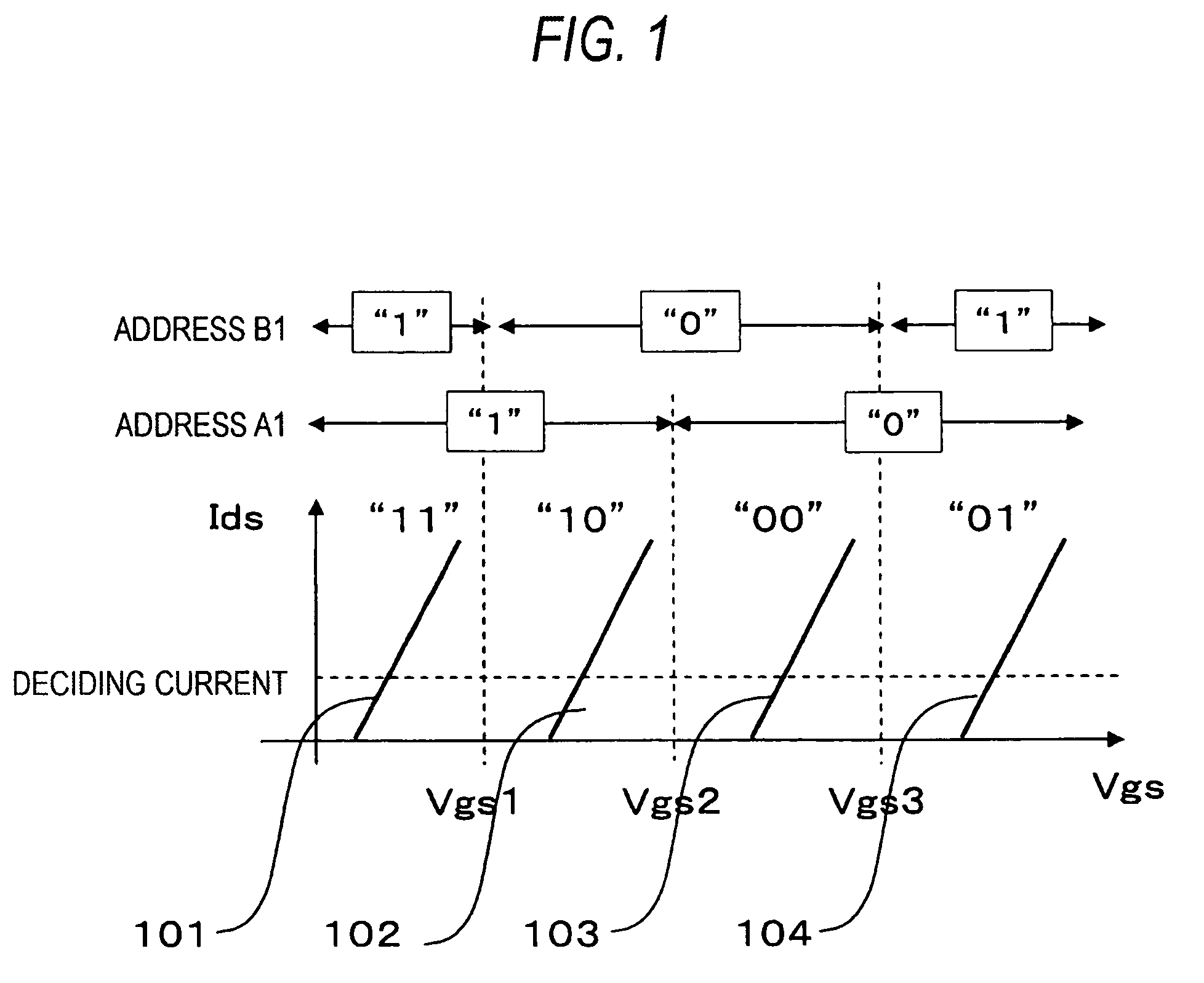
[0085]FIG. 7 is a chart showing setting of a threshold of a memory cell in a multivalued flash memory according to a second embodiment of the invention.

[0086]FIG. 7 shows a flash memory for storing four values in the same manner as FIG. 1, and a state in which “1” is stored in an address A1 and “1” is stored in an address B1 is set to be a state of the smallest threshold indicated as an Ids-Vgs characteristic 701 shown in FIG. 7, and a state in which “1” is stored in the address A1 and “0” is stored in the address B1 is set to be each threshold of an Ids-Vgs characteristic 702, a state in which “0” is stored in the address A1 and “0” is stored in the address B1 is set to be each threshold of an Ids-Vgs characteristic 703, and a state in which “0” is stored in the address A1 and “1” is stored in the address B1 is set to be each threshold of an Ids-Vgs characteristic 704 in ascending order of the threshold.

[0087]In...

third embodiment

[0091]Description will be given to a third embodiment according to the invention.

[0092]FIG. 8 is a diagram showing a structure of a flash memory according to the third embodiment of the invention.

[0093]The flash memory according to the embodiment is constituted by a flash memory chip 801 and a data saving memory 802 for once saving data in writing as shown in FIG. 8, and a separate memory chip from the flash memory chip 801 is used.

[0094]In contrast to the structure described in the first embodiment with reference to FIG. 3, in the embodiment, a region information storage region 810 having an electrically writable / erasable structure is employed in place of the region information storage region 310, and the same structure as that of a memory cell array 803 is desirable.

[0095]The other operations are the same as those in the first embodiment.

[0096]With such a structure, a high speed reading region in a mixing region and a normal reading operation region and a normal reading region in ...

fourth embodiment

[0105]Description will be given to a fourth embodiment according to the invention.

[0106]FIG. 9 is a diagram showing a structure of a flash memory according to the embodiment.

[0107]The flash memory according to the embodiment comprises a flash memory chip 901 and a data saving memory 902 for once saving data in writing, and the data saving memory 902 is a separate memory chip from the flash memory chip 901 as shown in FIG. 9.

[0108]A memory cell array 903 includes a plurality of multivalued memory cells capable of storing 2-bit information. In the memory cell array 903, there are a mixing region 904 having a high speed reading region and a region having a normal reading speed which are mixed and a normal reading operation region 905 having a normal reading speed. In the embodiment, a discrete arrangement is carried out and the threshold of the memory cell and the region are set as described with reference to FIG. 1.

[0109]Furthermore, there are provided an erasing control circuit 906 f...


PUM


Abstract

A memory cell array is logically divided into a plurality of regions having different reading speeds, the respective regions having the different reading speeds include region information storage regions for storing region information in which at least two addresses present in the memory cell at the same time are set to be different regions, a reading control circuit is constituted to carry out a reading operation by determining any of the divided regions which is to be read, selecting an optimum reading method and controlling the reading circuit based on the region information stored in the region information storage region, and an address which can be read in a short time in multivalued information stored in one memory cell is set to be a high speed reading region and is distinguished from regions having the other reading speeds. Consequently, it is possible to efficiently write and read information of 2 bits or more in one memory cell array without reducing a using efficiency of the memory cell array.

Description

BACKGROUND OF THE INVENTION[0001]1. Field of the Invention[0002]The present invention relates to a nonvolatile semiconductor storage apparatus and a method of driving the same, and more particularly to a driving operation of an electrically writable / erasable nonvolatile semiconductor storage apparatus capable of storing information of 2 bits or more in one memory cell.[0003]2. Description of the Related Art[0004]An electrically writable / erasable nonvolatile semiconductor storage apparatus (flash memory) has spread for storing a program code. In recent years, in addition to the uses, uses for storing mass data such as image data, voice data or animation data have been demanded and a further increase in a capacity has been required.[0005]In a system such as a cell phone, moreover, there has been demanded a flash memory capable of implementing, in one chip, a storage of a program code demanded to have an increase in a reading speed and various data required to have an increase in a cap...

Claims


Application Information

Patent Timeline
Patent Type & Authority Patents(United States)
IPC IPC(8): G11C11/34
CPCG11C11/5642G11C16/26G11C16/32G11C2211/5641
Inventor NAKAYAMA, MASAYOSHIMIYOSHI, ASAKOYAMAHIRA, SEIJI
Owner PANASONIC CORP
Why Eureka
Try Eureka