Device for controlling on die termination

a technology of termination device and die, applied in the direction of logic circuit coupling/interface arrangement, pulse technique, instruments, etc., can solve the problems of difficult control of the active period of the odt, signal reflection error can occur, and inability to obtain appropriate matching

Active Publication Date: 2008-03-11
SK HYNIX INC
View PDF8 Cites 34 Cited by
  • Summary
  • Abstract
  • Description
  • Claims
  • Application Information

AI Technical Summary

Benefits of technology

[0012]It is, therefore, an object of the present invention to provide an on die termination (ODT) control device for determining an active period of an ODT circuit by using latency information to thereby flexibly control a termination impedance of the ODT circuit.

Problems solved by technology

If the termination impedance is not appropriately matched, a signal reflection error can occur, i.e., a transferred signal can be reflected back.
However, if an external fixed resistor is provided, an appropriate matching may not be obtained due to aging of an integrated circuit, temperature variations or manufacturing process variations.
If the clock frequency of the semiconductor memory device grows shorter, it is difficult to control an active period of the ODT enable signal ODT_EN corresponding to the shortened clock frequency.
As a result, the conventional ODT control device cannot accurately measure the termination impedance of the semiconductor memory device.

Method used


Image

  • Device for controlling on die termination
  • Device for controlling on die termination
  • Device for controlling on die termination

Examples


Embodiment Construction

[0021]Hereinafter, an on die termination (ODT) control device in accordance with the present invention will be described in detail referring to the accompanying drawings.

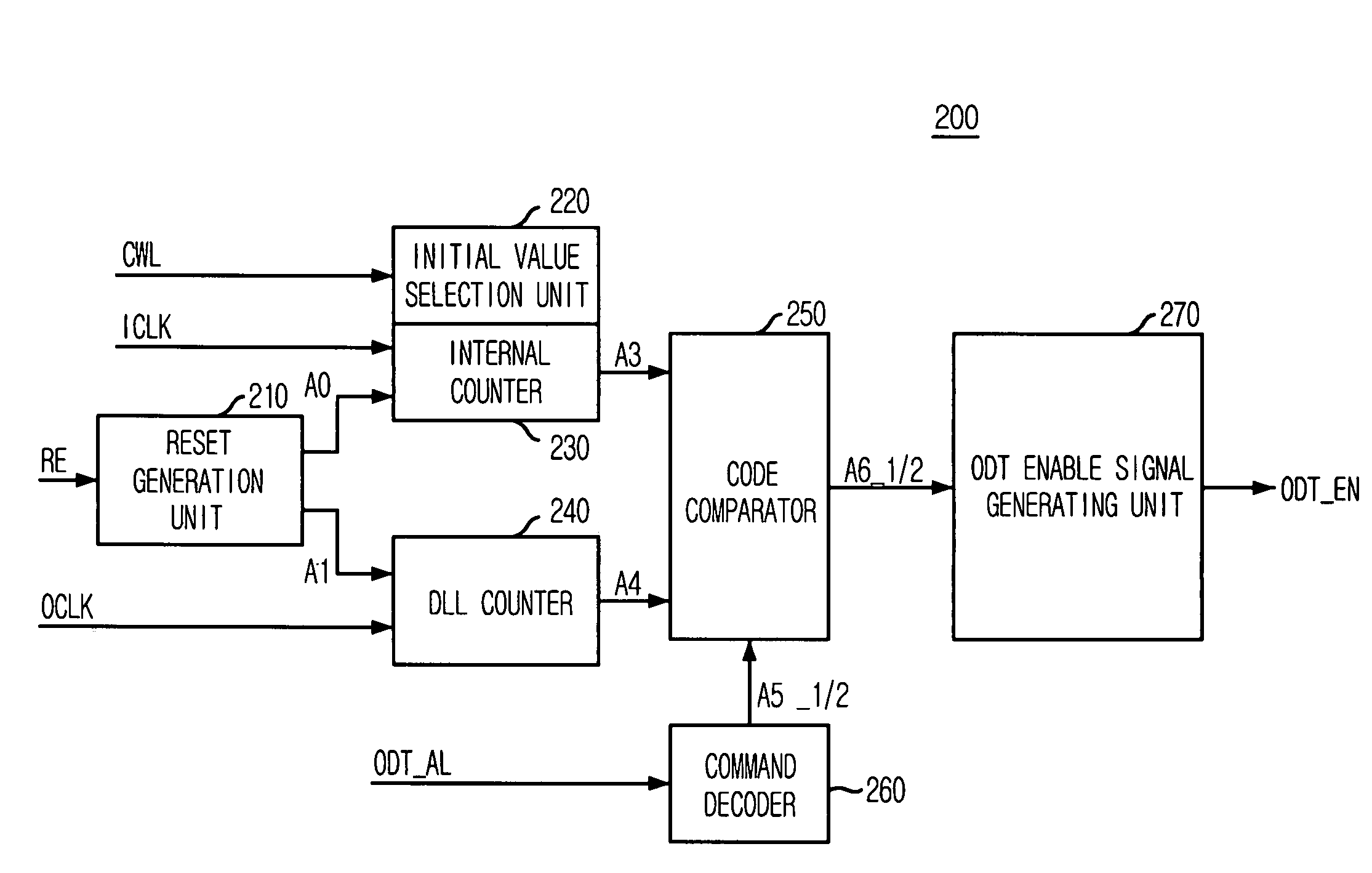
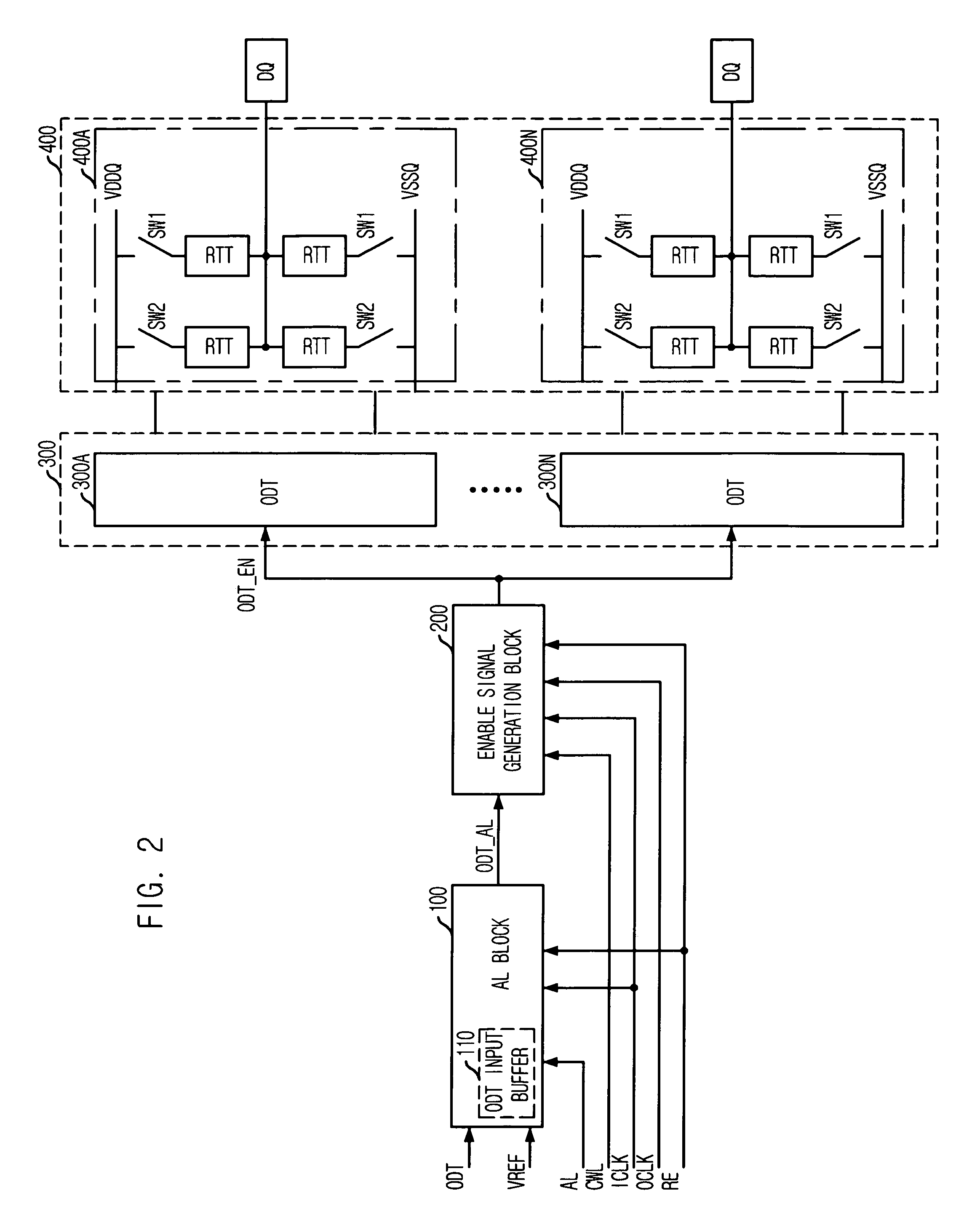
[0022]FIG. 2 is a block diagram showing an ODT control device in accordance with an embodiment of the present invention.

[0023]The ODT control device includes an additive latency (AL) block 100, an enable signal generation block 200, an ODT block 300 and a termination resistor block 400.

[0024]The AL block 100 performs a buffering operation of an ODT control signal ODT and a reference voltage VREF and receives an additive latency signal AL, an internal clock ICLK and a reset signal RE to generate a latency control signal ODT_AL. The additive latency signal AL defines how many clocks are required from a point of loading a read command or a write command to a point of recognizing them during a read or a write operation.

[0025]The enable signal generation block 200 receives the latency control signal ODT_AL, a column addr...


PUM


Abstract

An on die termination (ODT) control device includes a latency block for buffering an ODT control signal to output a latency control signal by selecting one of a plurality of intermediate control signals, which are generated by sequentially delaying the buffered ODT control signal in synchronization with an internal clock, based on first latency information; an enable signal generation block for comparing a first control signal with a second control signal in response to the latency control signal to thereby produce an ODT enable signal based on the compared result; and an ODT block for controlling a termination impedance based on the ODT enable signal.

Description

TECHNICAL FIELD[0001]The present invention relates to a device for controlling an on die termination (ODT); and, more particularly, to an ODT control device for determining an active period of an ODT circuit by using latency information.BACKGROUND[0002]Recently, various new technologies have been developed for improving data transferring speed of a double data rate (DDR) memory device. For instance, an off chip driver (OCD) calibration technology has been introduced to a specification of the DDR memory device by the JEDEC (Joint Electron Engineering Council) in order to adjust an impedance of a data output unit of the DDR memory device.[0003]The optimum impedance of a data output driver for a current system is detected by measuring a voltage or a current which flows from an external circuit such as a chip set to the data output driver so that an impedance of the data output driver is adjusted to the optimum impedance. For this purpose, a DDR2 synchronous semiconductor memory device ...

Claims


Application Information

Patent Timeline
Patent Type & Authority Patents(United States)
IPC IPC(8): H03K19/003
CPCG11C5/063G11C7/1048G11C7/1051G11C7/1066G11C29/02G11C29/025G11C29/028G11C29/50008H04L25/0278H04L25/0298G11C2207/2254G11C7/1078G11C7/22H03K19/017545
Inventor KIM, KYUNG-HOON
Owner SK HYNIX INC
Why Eureka
Try Eureka