Method and device for controlled cleaving process

a technology of controlled cleaving and process, which is applied in the direction of microstructural devices, coatings, microstructures, etc., can solve the problems of difficult separating or cutting extremely hard and/or brittle materials such as diamonds or glass, and cannot be used to provide precision separation in the substrate for the manufacture of fine tools and assemblies,

Inactive Publication Date: 2008-03-25
SILICON GENERAL CORPORATION
View PDF266 Cites 53 Cited by
  • Summary
  • Abstract
  • Description
  • Claims
  • Application Information

AI Technical Summary

Benefits of technology

[0009]According to the present invention, an improved technique for removing a thin film of material from a substrate using a controlled cleaving action is provided. This technique allows an initiation of a cleaving process on a substrate using a single or multiple cleave region(s) through the use of controlled energy (e.g., spatial distribution) and selected conditions to allow an initiation of a cleave front(s) and to allow it to propagate through the substrate to remove a thin film of material from the substrate.
[0011]In an alternative embodiment, the present invention provides a process for forming a film of material from substrates. The process includes providing a bulk substrate (e.g., silicon) comprising an upper surface. The process also includes forming a cleaving layer overlying the upper surface. The process also includes forming a material layer (e.g., epitaxial silicon) overlying the cleaving layer. Next, particles (e.g., hydrogen, helium, deuterium, or any other light atomic mass particles and the like) are introduced into the cleaving layer. These particles enhance the present cleaving action, which is described below. Energy is provided using a fluid to a selected region of the cleaving layer to initiate and maintain a controlled cleaving action at the cleaving layer, whereupon the cleaving action is made using a propagating cleave front to free the material layer from the bulk substrate. In a specific embodiment, cleaving occurs at or within the cleaving layer.
[0014]Numerous benefits are achieved over pre-existing techniques using the present invention. In particular, the present invention uses controlled energy and selected conditions to preferentially cleave a thin film of material from a donor substrate which includes multi-material sandwiched films. This cleaving process selectively removes the thin film of material from the substrate while preventing a possibility of damage to the film or a remaining portion of the substrate. Accordingly, the remaining substrate portion can be re-used repeatedly for other applications.
[0015]Additionally, the present invention uses a relatively low temperature during the controlled cleaving process of the thin film to reduce temperature excursions of the separated film, donor substrate, or multi-material films according to other embodiments. In most cases, the controlled cleaving process can occur at, for example, room temperature, as well as others. This lower temperature approach allows for more material and process latitude such as, for example, cleaving and bonding of materials having substantially different thermal expansion coefficients. In other embodiments, the present invention limits energy or stress in the substrate to a value below a cleave initiation energy, which generally removes a possibility of creating random cleave initiation sites or fronts. This reduces cleave damage (e.g., pits, crystalline defects, breakage, cracks, steps, voids, excessive roughness) often caused in pre-existing techniques. Moreover, the present invention reduces damage caused by higher than necessary stress or pressure effects and nucleation sites caused by the energetic particles as compared to pre-existing techniques. Depending upon the embodiment, one or more of these advantages, as well as others, may exist.

Problems solved by technology

This technique, however, is often extremely “rough” and cannot generally be used for providing precision separations in the substrate for the manufacture of fine tools and assemblies.
Additionally, the saw operation often has difficulty separating or cutting extremely hard and / or brittle materials such as diamond or glass.
Although the techniques described above are satisfactory, for the most part, as applied to cutting diamonds or household glass, they have severe limitations in the fabrication of small complex structures or precision workpieces.
For instance, the above techniques are often “rough” and cannot be used with great precision in fabrication of small and delicate machine tools, electronic devices, or the like.
Additionally, the above techniques may be useful for separating one large plane of glass from another, but are often ineffective for splitting off, shaving, or stripping a thin film of material from a larger substrate.
Furthermore, the above techniques may often cause more than one cleave front, which join along slightly different planes, which is highly undesirable for precision cutting applications.
Other processing techniques such as the use of a release layer have also had limited success.
Such release layer techniques often require wet chemical etching, which is often undesirable in many state of art applications.

Method used


Image

  • Method and device for controlled cleaving process
  • Method and device for controlled cleaving process
  • Method and device for controlled cleaving process

Examples


Embodiment Construction

[0032]The present invention provides a technique for removing a thin film of material from a substrate while preventing a possibility of damage to the thin material film and / or a remaining portion of the substrate. The thin film of material is attached to or can be attached to a target substrate to form, for example, a silicon-on-insulator wafer. The thin film of material can also be used for a variety of other applications. The invention will be better understood by reference to the Figs. and the descriptions below.

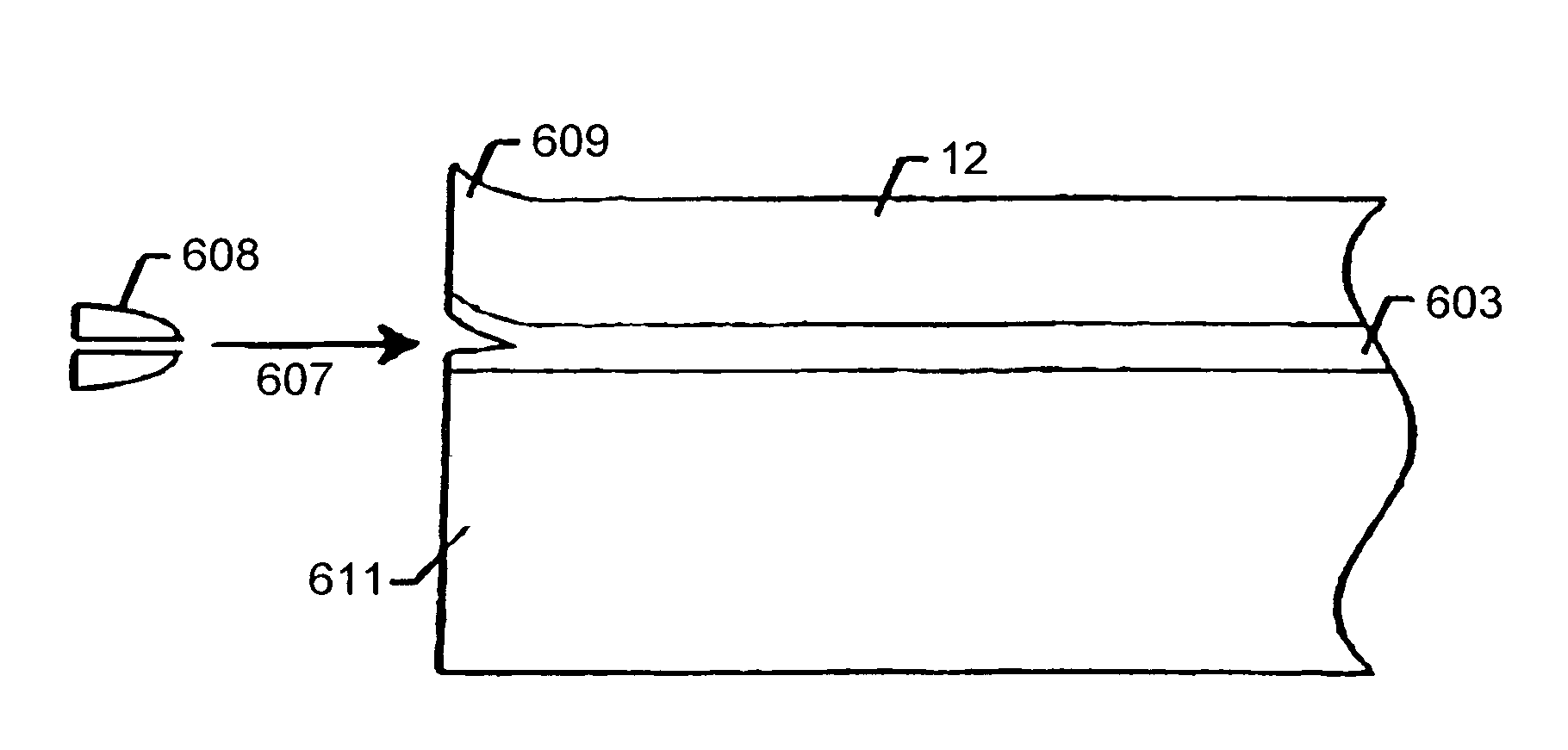
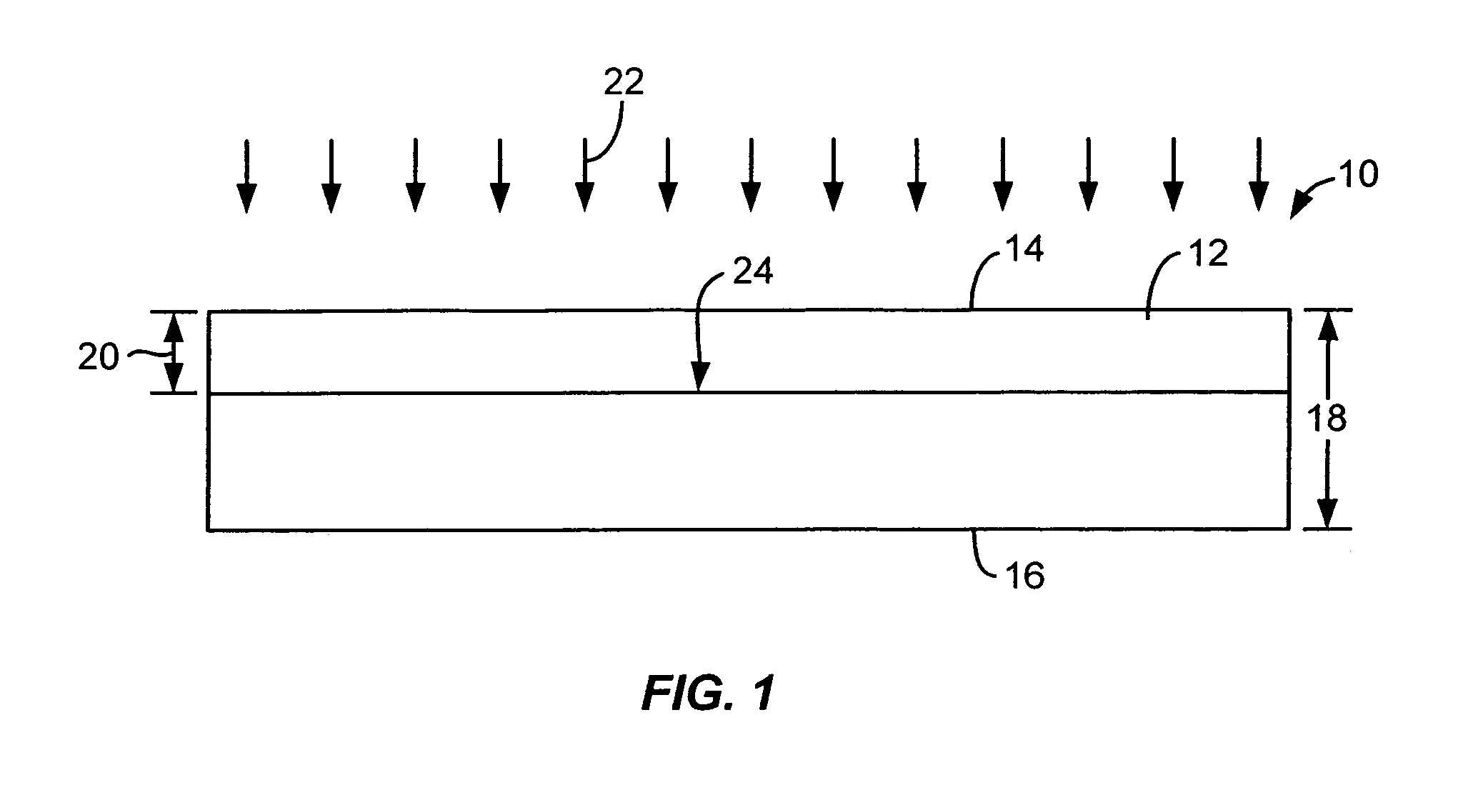
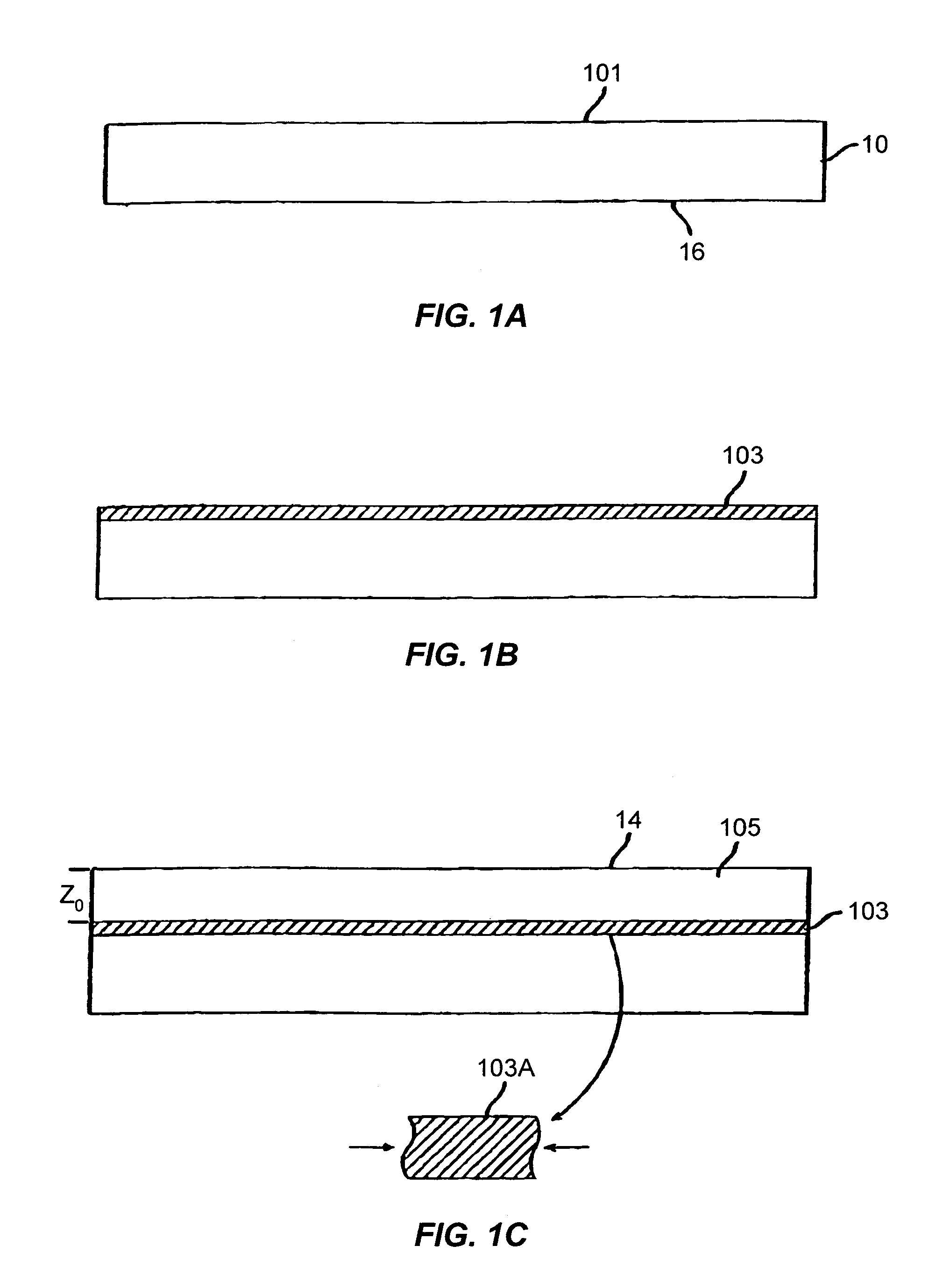
[0033]FIG. 1 is a simplified cross-sectional view diagram of a substrate 10 according to the present invention. The diagram is merely an illustration and should not limit the scope of the claims herein. As merely an example, substrate 10 is a silicon wafer which includes a material region 12 to be removed, which is a thin relatively uniform film derived from the substrate material. The silicon wafer 10 includes a top surface 14, a bottom surface 16, and a thickness 18. S...


PUM

PropertyMeasurementUnit
pressureaaaaaaaaaa
surface roughnessaaaaaaaaaa

Abstract

A technique for forming a film of material (12) from a donor substrate (10). The technique has a step of forming a stressed region in a selected manner at a selected depth (20) underneath the surface. An energy source such as pressurized fluid is directed to a selected region of the donor substrate to initiate a controlled cleaving action of the substrate (10) at the selected depth (20), whereupon the cleaving action provides an expanding cleave front to free the donor material from a remaining portion of the donor substrate.

Description

CROSS-REFERENCES TO RELATED APPLICATIONS[0001]This application is a continuation of U.S. patent application Ser. No. 10 / 268,918, filed Oct. 9, 2002, now U.S. Pat. No. 6,790,747, which is a continuation of U.S. patent application Ser. No. 09 / 790,026, filed Feb. 20, 2001, now U.S. Pat. No. 6,486,041, which is a continuation of U.S. patent application Ser. No. 09 / 480,979, filed Jan. 10, 2000, now U.S. Pat. No. 6,284,631, which is a continuation of U.S. patent application Ser. No. 09 / 370,975, filed Aug. 10, 1999, now U.S. Pat. No. 6,033,974, which is a continuation-in-part of U.S. patent application Ser. No. 09 / 313,959, filed May 18, 1999, now U.S. Pat. No. 6,291,313, which is a continuation of U.S. patent application Ser. No. 09 / 026,027, filed Feb. 19, 1998, now U.S. Pat. No. 5,994,207, which claims the benefit of U.S. Provisional Application No. 60 / 046,276, filed May 12, 1997 commonly owned and hereby incorporated by reference for all purposes.BACKGROUND OF THE INVENTION[0002]The pres...

Claims


Application Information

Patent Timeline
Patent Type & Authority Patents(United States)
IPC IPC(8): H01L21/30H01L21/46B81C1/00H01L21/22H01L21/38
CPCB81C1/0038H01L21/26506H01L21/76254B81C2201/0191B81C2201/0192H01L21/2658
Inventor HENLEY, FRANCOIS J.CHEUNG, NATHAN
Owner SILICON GENERAL CORPORATION
Why Eureka
Try Eureka