Apparatus for performing high frequency electronic package testing

a technology for electronic packages and apparatuses, which is applied in the testing/measurement of individual semiconductor devices, semiconductor/solid-state devices, instruments, etc., can solve the problems of poor quality of probe connection, difficult connection between test equipment and ic connections on the package, and inability to achieve very high bandwidth interface between test equipment and bga packages. to achieve the effect of accurate testing

Inactive Publication Date: 2008-03-25
XILINX INC
View PDF6 Cites 7 Cited by
  • Summary
  • Abstract
  • Description
  • Claims
  • Application Information

AI Technical Summary

Benefits of technology

[0010]The present invention solves the above-described problems by providing a test methodology that enables electronic packaging having an interface structure to be accurately tested at very high frequencies. The test methodology employs the use...

Problems solved by technology

The main obstacle with producing high accuracy tests is the lack of a very high bandwidth interface between the test equipment and BGA package.
Connections between the test equipment to the IC connections on the ...

Method used


Image

  • Apparatus for performing high frequency electronic package testing
  • Apparatus for performing high frequency electronic package testing
  • Apparatus for performing high frequency electronic package testing

Examples


Embodiment Construction

[0018]In the following description of the embodiments, reference is made to the accompanying drawings that form a part hereof, and in which is shown by way of illustration the specific embodiments in which the invention may be practiced. It is to be understood that other embodiments may be utilized because structural changes may be made without departing from the scope of the present invention.

[0019]An apparatus of an embodiment of the present invention provides for performing high frequency electronic package testing. The embodiment enables electronic packages having an interface structure to be accurately tested at very high frequencies.

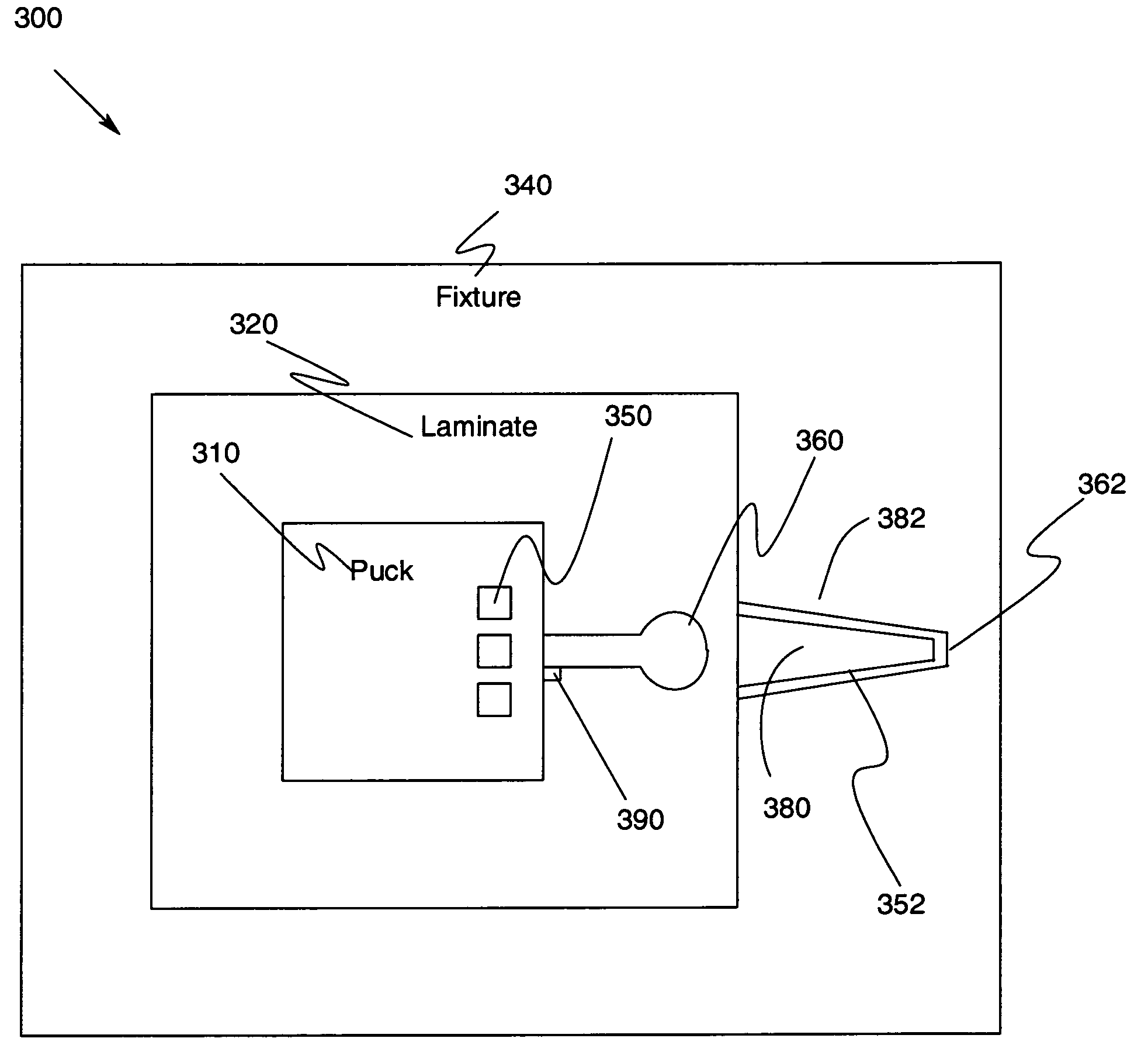
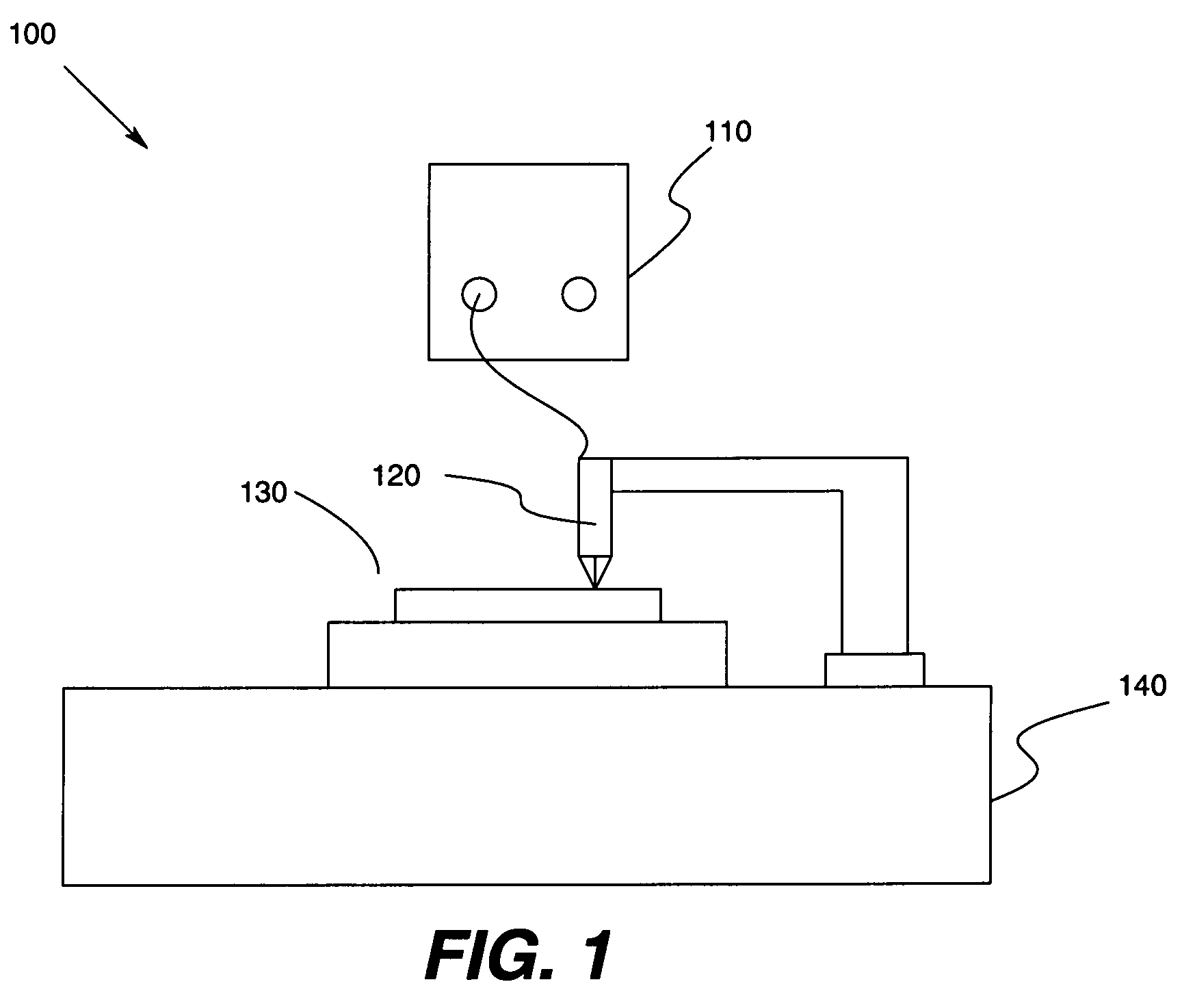
[0020]FIG. 1 illustrates a test system 100 that may be used to perform high frequency electronic package testing of electronic devices according to an embodiment of the present invention. The test system 100 includes a network analyzer 110 that may be electrically connected to a coaxial test probe 120. The coaxial test probe 120 is configured to es...


PUM


Abstract

Various apparatus for performing high frequency electronic package testing are disclosed. A test fixture assembly includes an electronics package having an interface structure, a mock-up IC, coupled to the interface structure for providing circuit connections, and a fixture board, coupled to the interface structure, wherein at least one of the fixture board and mock-up IC includes high frequency probe pads for providing a signal and ground point for high bandwidth test probing. Raw measurements are used for validation of the electronic package specifications when adequate test fixture bandwidth is available or included into circuit simulations models when a minimal phase error is acceptable, else phase and loss corrections are applied to the measurements.

Description

FIELD OF THE INVENTION[0001]This disclosure relates in general to testing of electronic devices, and more particularly to an apparatus for performing high frequency electronic package testing.BACKGROUND[0002]The semiconductor industry has seen a major shift from leads to balls and from wires to bumps. This requires infrastructure developments and promises new opportunities. Ball grid array (BGA) packages are increasingly found in products including personal computers, portable communications devices, workstations / servers, mid-range and high-end computers, network and telecommunications systems, and even automotive applications. More specifically, BGA packages are being used in high speed circuits such as processors, application specific integrated circuits (ASICs), storage controllers, video controllers, programmable logic devices (PLDs), field programmable gate array (FPGA), etc.[0003]Today's BGA packages boast high clock speeds, fine pitch structures and high pin-counts. When thes...

Claims


Application Information

Patent Timeline
IPC IPC(8): H01L23/58
CPCG01R1/045H01L2924/3011H01L2224/73204H01L2224/73265H01L2224/16225H01L2224/32225H01L2224/48227H01L2924/15311H01L23/66H01L2224/48091H01L2924/00012H01L2924/00H01L2924/00014H01L24/73H01L2924/14H01L2224/05573H01L2224/13025H01L2224/0554H01L2224/05599H01L2224/0555H01L2224/0556
Inventor DEGERSTROM, MICHAEL J.BIBEE, MATTHEW L.HULSE, DANIEL V.
Owner XILINX INC
Why Eureka
Try Eureka