Configurable logic component without a local configuration memory and with a parallel configuration bus

a technology of configuration memory and configuration component, which is applied in the direction of computation using denominational number representation, instruments, pulse techniques, etc., can solve the problems of high degree of configuration expenditure for logic cells and the associated connection network, inability to change configuration with real-time applications, and area requirements, so as to increase operational reliability, cost-effective effect of manufacturing an integrated circui

Inactive Publication Date: 2008-03-25
INFINEON TECH AG
View PDF13 Cites 6 Cited by
  • Summary
  • Abstract
  • Description
  • Claims
  • Application Information

AI Technical Summary

Benefits of technology

[0017]By preventing a sequential transmission of data it is possible to dispense with buffering configuration data in local configuration memories which are arranged within the configurable logic component.
[0055]The devices and methods according to the invention support the rapid configuration changeover and at the same time facilitate the multiple use of the programmable logic component in real-time requirements. After a very short break in operation for the reprogramming, the data can be further processed. At the same time, the data can be buffered during the configuration changeover in the flip-flops of the configurable logic cells or in a data RAM (Random Access Memory).

Problems solved by technology

The latter exhibit a maximum level of flexibility and therefore have a high degree of expenditure on configuration for the logic cells and the associated connection network.
A configuration changeover is therefore incompatible with real-time applications.
The most important disadvantages of the described solution are the economic reasons (area requirement) and the limited miniaturizability of the system structure.
The technical disadvantages of this solution are the limited bandwidth for the exchange of data and the continuing need to buffer it locally.
However, the significant and very expensive disadvantage of this solution is the need to combine two different semiconductor technologies on one chip and to make available a semiconductor technology which optimizes both EEPROM cells and configurable cells.

Method used


Image

  • Configurable logic component without a local configuration memory and with a parallel configuration bus
  • Configurable logic component without a local configuration memory and with a parallel configuration bus
  • Configurable logic component without a local configuration memory and with a parallel configuration bus

Examples


Embodiment Construction

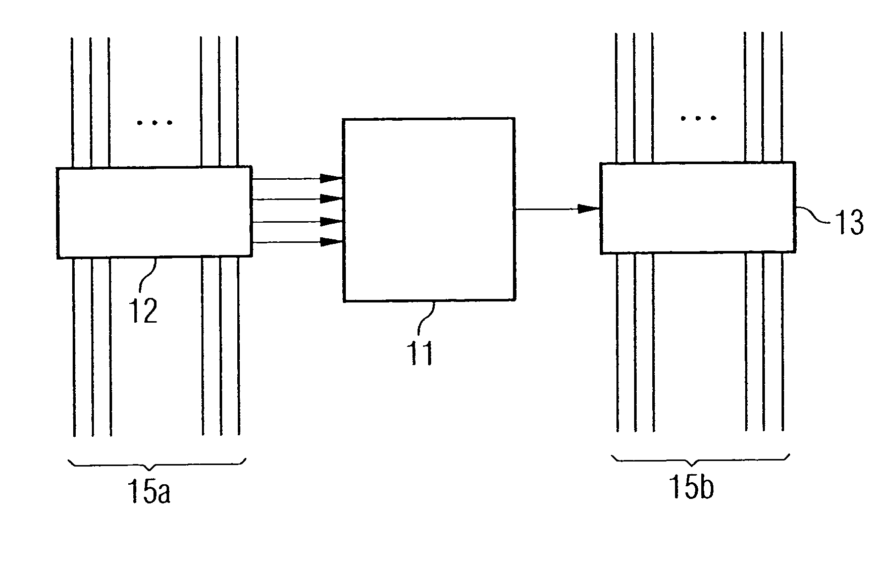
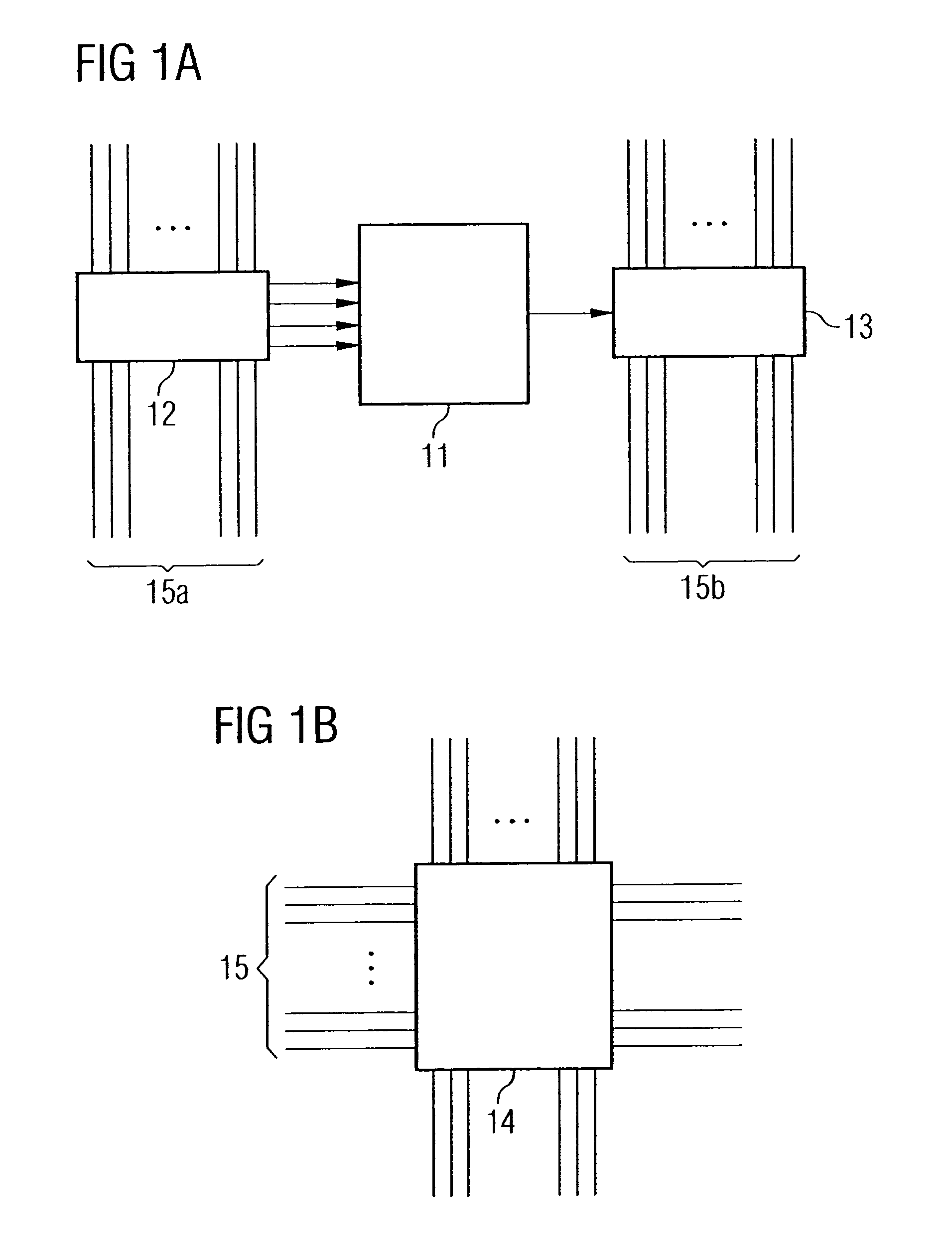
[0062]The four cell types which occur in general within a logic component, for example a programmable logic component or an FPGA, are illustrated in FIGS. 1a and 1b. Configurable logic cells 11 are used for signal processing at the bit level. Configurable tap cells 12 tap as many signals as the logic cell 11 has inputs from a data bus 15a. Configurable feed cells 13 feed the output signal of the logic cell 11 to a further data bus 15b. Configurable coupling cells 14 are matrices for the optional and bidirectional switching of signal paths (wiring) in the connection network of a logic component 30.

[0063]A typical implementation of a configurable logic cell 11 uses look-up tables (lut). In what follows, a look-up table (lut4) with four input signals and an output signal is assumed as an example. The table requires 16 configuration signals for non-restricted configurability. The flip-flop connected downstream and the multiplexer require approximately 5 configuration bits in total. The ...


PUM


Abstract

A configurable logic component (30) does not have a local configuration memory. The configuration of the configurable logic component is defined by applied voltages. The configuration voltages are advantageously generated in an external configuration memory (2). In one preferred refinement, a memory chip (20) (for example EEPROM) and the inventive logic component without a configuration memory (30) are mounted face-to-face. An intermediate, structured solder layer (40) makes available a plurality of electrical connections.

Description

RELATED APPLICATIONS[0001]The present patent document claims the benefit of the filing date under 35 U.S.C. §119 of German Patent Application No. 10 2004 001 669.0, filed Jan. 12, 2004, which is hereby incorporated by reference.BACKGROUND[0002]The present invention relates to simplified devices and methods for quickly reprogramming a programmable logic component (PLD).[0003]Programmable logic components (PLD, programmable logic device) are general architectures which frequently have a very regular structure for logic operations. They contain a plurality of switches which can switch a plurality of signal paths. As a result, they only receive their specific function through configuration. A PLD (FIGS. 1a and 1b) is basically composed of configurable logic cells and a configurable connection network which permits the logic cells to be logically connected as desired. The configuration of the PLD relates here both to the logic cells and to the connection network, with the possibility of ...

Claims


Application Information

Patent Timeline
Patent Type & Authority Patents(United States)
IPC IPC(8): H03K19/173H03K19/177
CPCH03K19/1731H03K19/17704H03K19/17748H03K19/1776H03K19/17796
Inventor SCHEPPLER, MICHAELGRUBER, WOLFGANG
Owner INFINEON TECH AG
Why Eureka
Try Eureka