

Set of masks, method of generating mask data and method for forming a pattern
a mask and data technology, applied in the field of semiconductor device manufacturing, can solve the problems of difficult to form resist patterns, difficult to delineate circuit patterns, and low resolution of trim masks
- Summary
- Abstract
- Description
- Claims
- Application Information
AI Technical Summary
Benefits of technology
Problems solved by technology
Method used
Image

Examples
first embodiment
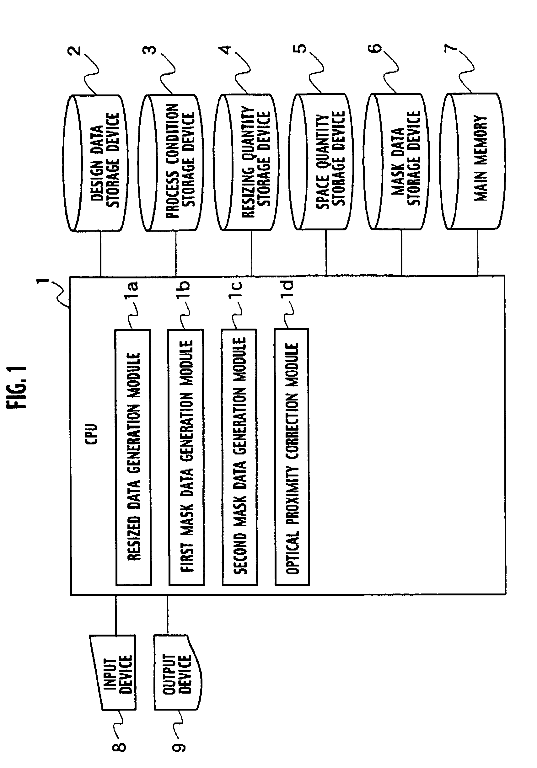
[0068]As shown in FIG. 1, a mask data generation system according to a first embodiment of the present invention includes a central processing unit (CPU) 1, design data storage device 2, a process condition storage device 3, a resizing quantity storage device 4, a space quantity storage device 5, a mask data storage device 6, a main memory 7, an input device 8, and an output device 9.
[0069]The process condition storage device 3 stores process conditions, such as exposure conditions and ion implantation conditions, for delineating a circuit pattern of a semiconductor integrated circuit (IC). Here, exposure conditions also include a minimum line width and a minimum space width with which a pattern can be optically resolved by a projection exposure system used in the photolithography processes, as an example.
[0070]The design data storage device 2 stores in advance design data. The design data is drawn design patterns that correspond to patterns having desired shapes on a semiconductor ...
second embodiment
[0120]As shown in FIG. 23, a mask data generation system according to the second embodiment of the present invention includes a central processing unit (CPU) 1x, a design data storage device 2, a process condition storage device 3, a resizing quantity storage device 4, a space quantity storage device 5, a mask data storage device 6, a main memory 7, an input device 8, and an output device 9.
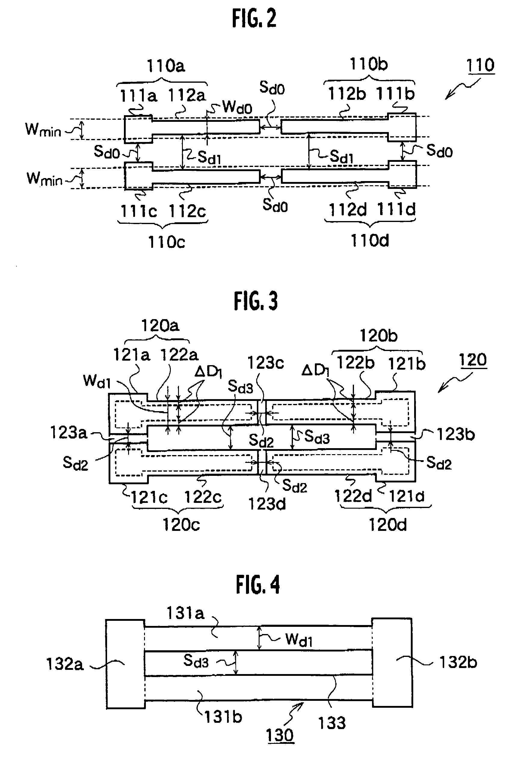
[0121]The design data storage device 2 stores design data 210 shown in FIG. 24 instead of the design data 110 shown in FIG. 2. The design data 210 includes four design patterns 110a, 110b, 110c, and 110d for forming desired process-target film patterns on a semiconductor substrate, the same as design data 110. The design patterns 110a, 110b, 110c, and 110d all have a line symmetrical (mirror symmetrical) relationship and have the same shape with one another. The two thin line portion 112a and 112b are separated from each other by the space width Sd6 therebetween in the X-axis direction. The two t...
first modification
[0158]A method for forming a pattern according to a first modification of the second embodiment of the present invention is different from the method for forming a pattern according to the second embodiment in that a TF process utilizing a thermal plastic deformation characteristic of a resist is used as shown in FIGS. 44A to 45, instead of the overcoat method shown in FIGS. 38 to 41.
[0159](a) By subjecting the second resist pattern 35b shown in FIGS. 37A and 37B to heat treatment, a second resist pattern 35c is delineated which has window portions 36i, 36j, 36k, and 36l as shown in FIGS. 44A and 44B. The window portions 36i and 36j are obtained by isotropically reducing the window portions 36e and 36f, respectively, each by a space width reducing quantity ΔL2 (=ΔD2) and each have a side with a length of the target space width Sp6 in the Y-axis direction. The window portions 36k and 36l are obtained by isotropically reducing the window portions 36g and 36h, respectively, each by ΔL2...
PUM
| Property | Measurement | Unit |
|---|---|---|
| widths | aaaaa | aaaaa |
| thickness | aaaaa | aaaaa |
| thickness | aaaaa | aaaaa |
Abstract
Description
Claims
Application Information