Cutting method and apparatus for ingot, wafer, and manufacturing method of solar cell

a manufacturing method and ingot technology, applied in the direction of sustainable manufacturing/processing, final product manufacturing, and under a protective fluid, can solve the problems of solar cell absorption of light, limited thickness, and near technical limit, and achieve the effect of shortening the time for cutting a single crystal ingot, high purity, and producing more and thinner wafers

Inactive Publication Date: 2008-04-01
Y Y L
View PDF5 Cites 17 Cited by
  • Summary
  • Abstract
  • Description
  • Claims
  • Application Information

AI Technical Summary

Benefits of technology

[0018]Accordingly, it is an object of the present invention to provide a method and an apparatus that specially shortens the time to cut a single crystal ingot to produce wafers.
[0019]It is another object of the present invention to provide a method and an apparatus that enables to produce more and thinner wafers from one ingot.
[0020]It is a further object of the present invention to provide a method and an apparatus that enable to produce wafers having a high purity and a high surface precision.

Problems solved by technology

However, the present status would be nearly at a technical limit.
The solar cell needs absorption of light and has a limitation in the thickness because of certain extent of required strength for processing.

Method used


Image

  • Cutting method and apparatus for ingot, wafer, and manufacturing method of solar cell
  • Cutting method and apparatus for ingot, wafer, and manufacturing method of solar cell
  • Cutting method and apparatus for ingot, wafer, and manufacturing method of solar cell

Examples


Embodiment Construction

[0050]The outline, principle and embodiments of the present invention are described as follows.

[0051]A method of the present invention comprises the following steps.

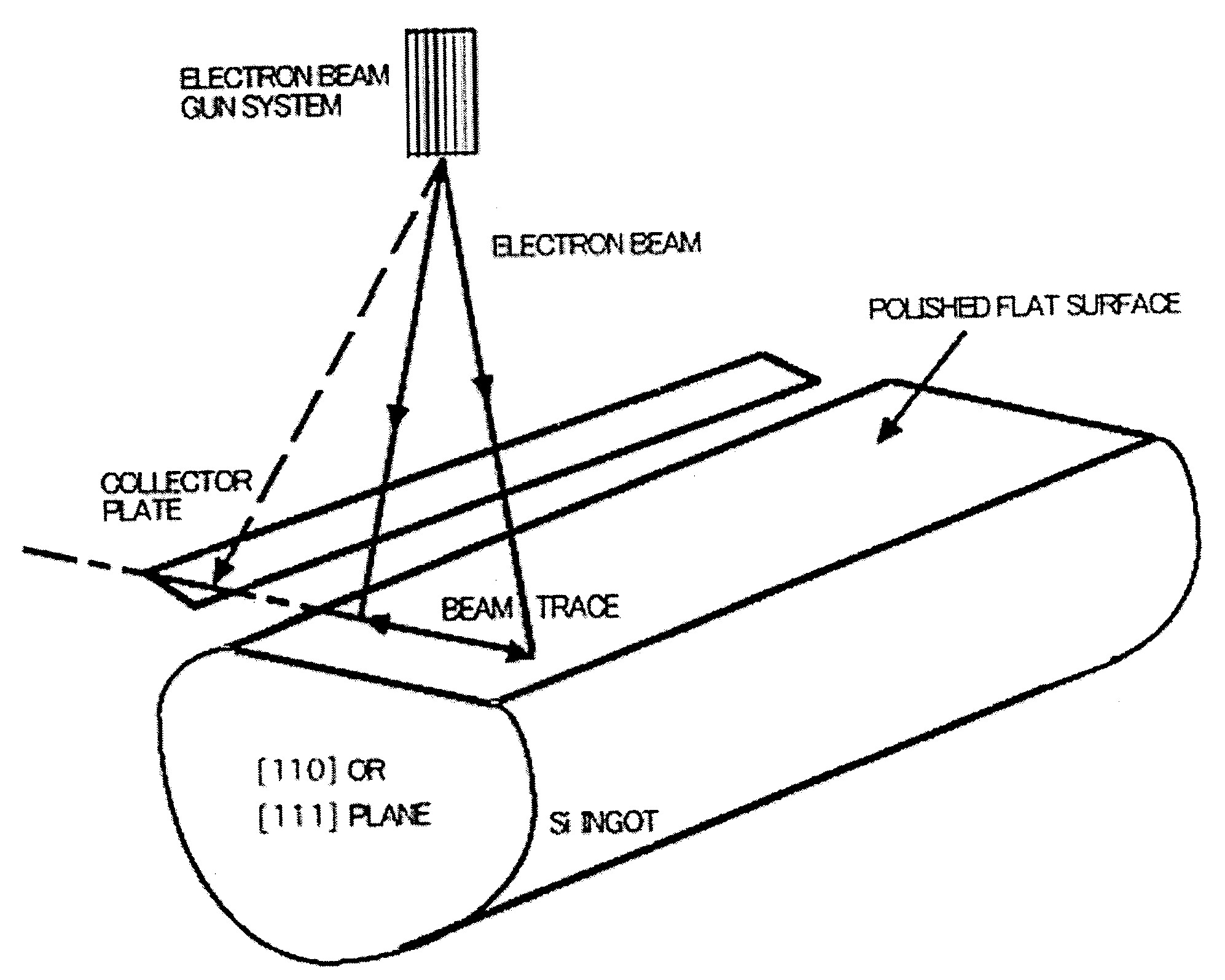
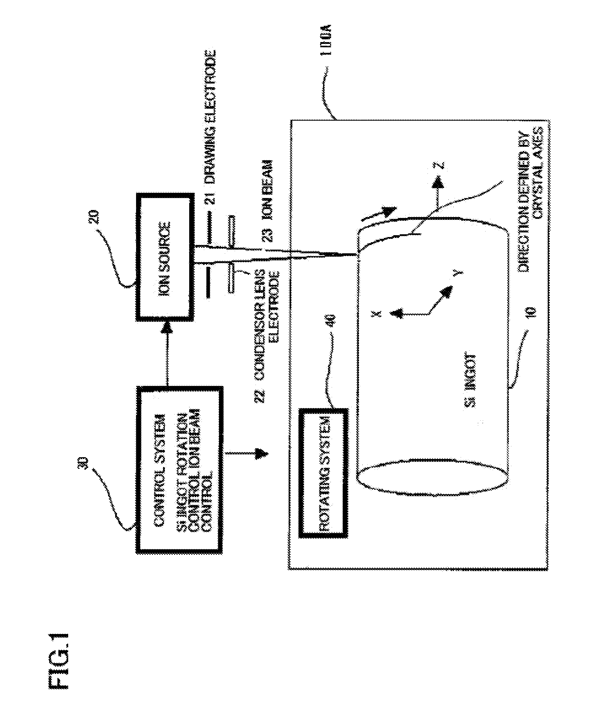
[0052]Step 1: Generating lattice defects in a (side) surface of a straightbody of a single crystal ingot along a direction defined by crystal axes, the direction corresponding to a cleavage plane in a crystal structure,

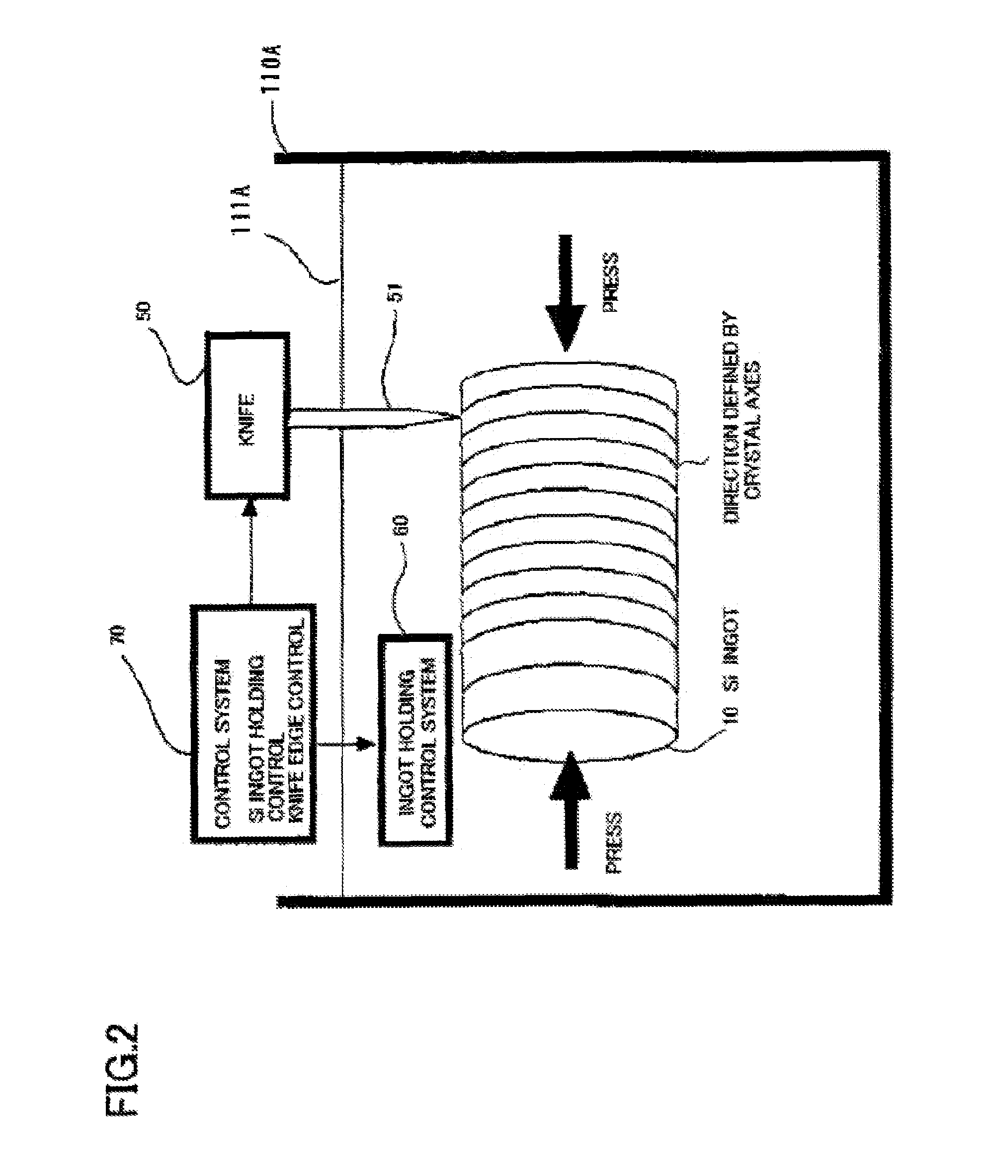
[0053]Step 2: Cleaving the ingot by applying a shock to a position where lattice defects have been generated by the Step 1, in the surface of the single crystal ingot, thereby cutting the ingot into a wafer having a cutting face formed as the cleavage plane.

[0054]In Step 1, the lattice defects are generated in the surface of the single crystal ingot along the direction defined by crystal axes, by irradiating the surface of the single crystal ingot with a working (or processing) beam along the direction defined by crystal axes.

[0055]The lattice defects may be generated in the surface of the single crystal i...


PUM

PropertyMeasurementUnit
lengthaaaaaaaaaa
lengthaaaaaaaaaa
thicknessaaaaaaaaaa

Abstract

Cutting method of ingot into wafers along cleavage plane. Onto surface of single crystal ingot 10 is implanted ion beam 23 to generate lattice defects in a direction defined by the crystal axes that corresponds to the cleavage plane. Cleavage is generated by applying a shock by a knife edge to the position of the lattice having a cutting face as a cleavage plane. Production time of waters is reduced with a more numbers of sliced wafers from one ingot.

Description

FIELD OF THE INVENTION[0001]The present invention relates to a method and apparatus for cutting a single crystal ingot, particularly a method and apparatus suitable for manufacturing a solar cell, and a wafer.BACKGROUND OF THE INVENTION[0002]Single crystal or polycrystal such as, for example, single crystal Si, amorphous Si or polycrystalline Si is widely used for an optoelectric conversion material (opto- voltaic material) to produce solar cells. Because, for example, amorphous Si has a forbidden band as wide as 1.7 eV and an absorption coefficient for visible light as large as ten times of single crystal Si. Additionally the single crystal Si is expensive. A solar cell made from ternary compounds of the chalcopyrite type attracts attention as a high efficiency solar cell material besides silicon, and CdS / CuInSe2 heterojunction polycrystal thin film or the like is eagerly studied, too.[0003]Amorphous Si or polycrystalline Si is made from a single crystal ingot as a base material. S...

Claims


Application Information

Patent Timeline
Patent Type & Authority Patents(United States)
IPC IPC(8): C30B13/02B28D5/04B26D7/08B28D5/00H01L21/304H01L31/00H01L31/04H01L31/18
CPCB28D5/00B28D5/0011H01L31/1804Y02B10/12Y02E10/547Y02B10/10Y10T83/0405Y02P70/50
Inventor YAMAGUCHI, SATARO
Owner Y Y L
Why Eureka
Try Eureka