

Reference clock receiver compliant with LVPECL, LVDS and PCI-Express supporting both AC coupling and DC coupling
a clock receiver and reference clock technology, applied in the field of reference clock receivers, can solve the problems that the conventional structure cannot meet the specifications of certain new industry standards, and achieve the effect of boosting the pair of differential outputs
- Summary
- Abstract
- Description
- Claims
- Application Information
AI Technical Summary
Benefits of technology
Problems solved by technology
Method used
Image

Examples
Embodiment Construction
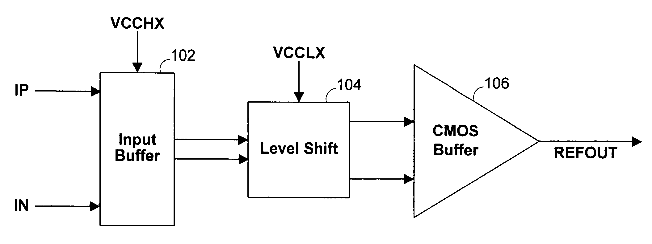
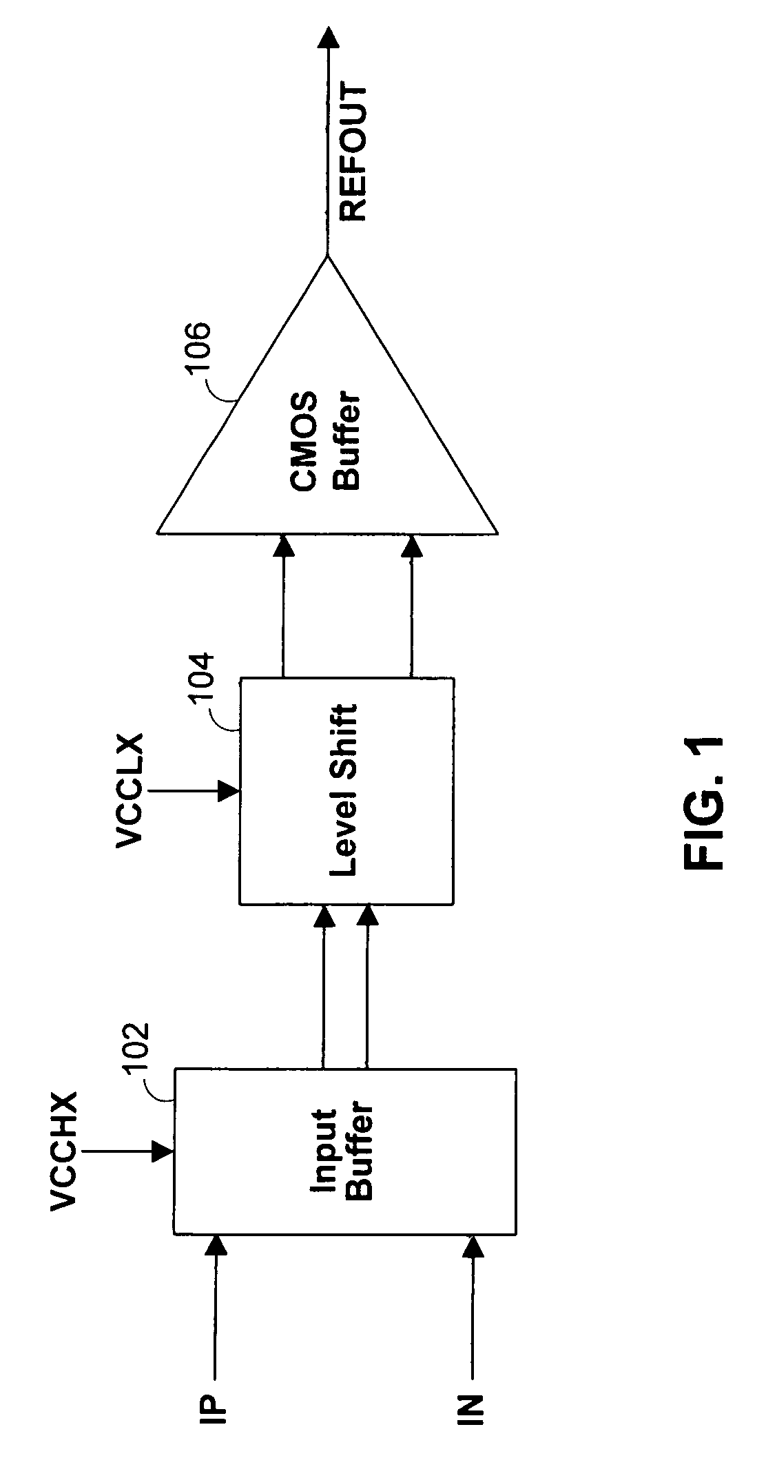
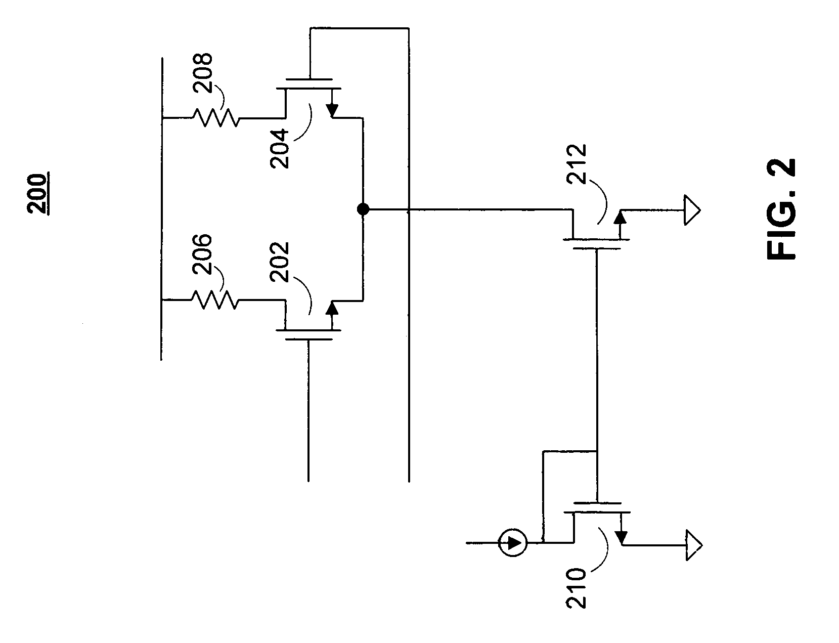
[0021]FIG. 3 shows a reference clock receiver 300 according to the invention. Reference clock receiver 300 preferably includes three stages: input buffer 301, level shifter 303 and differential-to-single ended converter 305.
[0022]Input buffer 301 preferably is formed from a PMOS-based differential pair of transistors 308 and 310 (together with resistors 310 and 312 and current mirror transistors 306 and 308) as opposed to the NMOS-based differential pair. By using a supply voltage VCCH=3.3 volts, the input common-mode range can go from about 0 volts to about 2.2 volts. This range is able to cover the voltage common-mode specifications of many industry standards such as PCI-Express (Vcm=0.25V˜0.55V), LVPECL (Vcm=1.8825V˜2.05V) and LVDS (Vcm=1.25 volts).
[0023]Receiver 300 preferably converts relatively high voltage levels to a core voltage level (1.2 volts). Because of this function, receiver 300 preferably uses thick oxide transistors 302, 304, 306 and 308. Thick oxide transistors ar...
PUM
 Abstract
Description
Claims
Application Information