Performing read and write operations in the same cycle for an SRAM device

a technology of read and write operation and sram device, which is applied in the field of memory devices, can solve the problems of more expensive dram and faster access to data by sram, and achieve the effects of reducing gap time, increasing overall cycle time, and increasing cycle tim

Active Publication Date: 2008-04-08
GSI TECH
View PDF4 Cites 35 Cited by
  • Summary
  • Abstract
  • Description
  • Claims
  • Application Information

AI Technical Summary

Benefits of technology

[0017]A gap time is generated between the read pulse and the write pulse so that write data is not mistakenly written into a memory cell intended to be read. The gap time between read pulse and the write pulse corresponds to the time between the falling edge of the read pulse and the rising edge of the write pulse. Because of different characteristics of p-mos transistors and n-mos transistors, the low-to-high delay and the high-to-low delay is diverse after several gates. When the falling edge slew rate of the read decoding signal is insufficient, such as after a long RC line, write data is mistakenly written into a read memory cell if the gap time is too short. In such a case, the gap time is increased at the cost of increasing the overall cycle time. Conversely, where the slew rate is sufficient to prevent unwanted overwriting, the gap time can be reduced to decrease the overall cycle time.

Problems solved by technology

SRAM provides faster access to data, but is more expensive than DRAM.

Method used


Image

  • Performing read and write operations in the same cycle for an SRAM device
  • Performing read and write operations in the same cycle for an SRAM device
  • Performing read and write operations in the same cycle for an SRAM device

Examples


Embodiment Construction

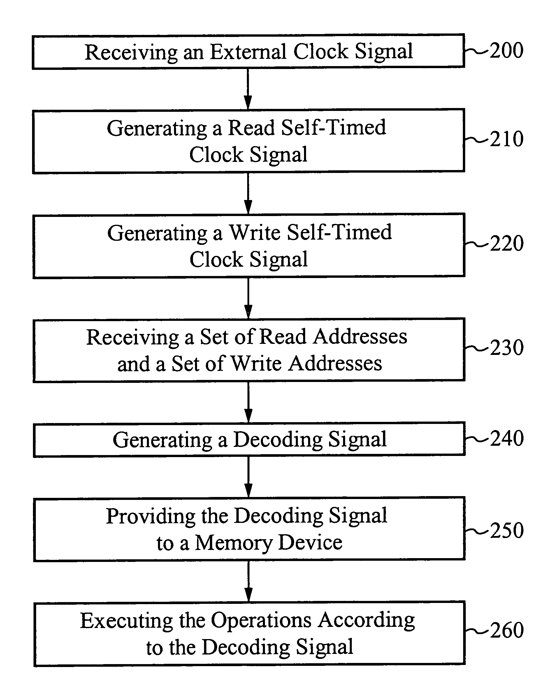
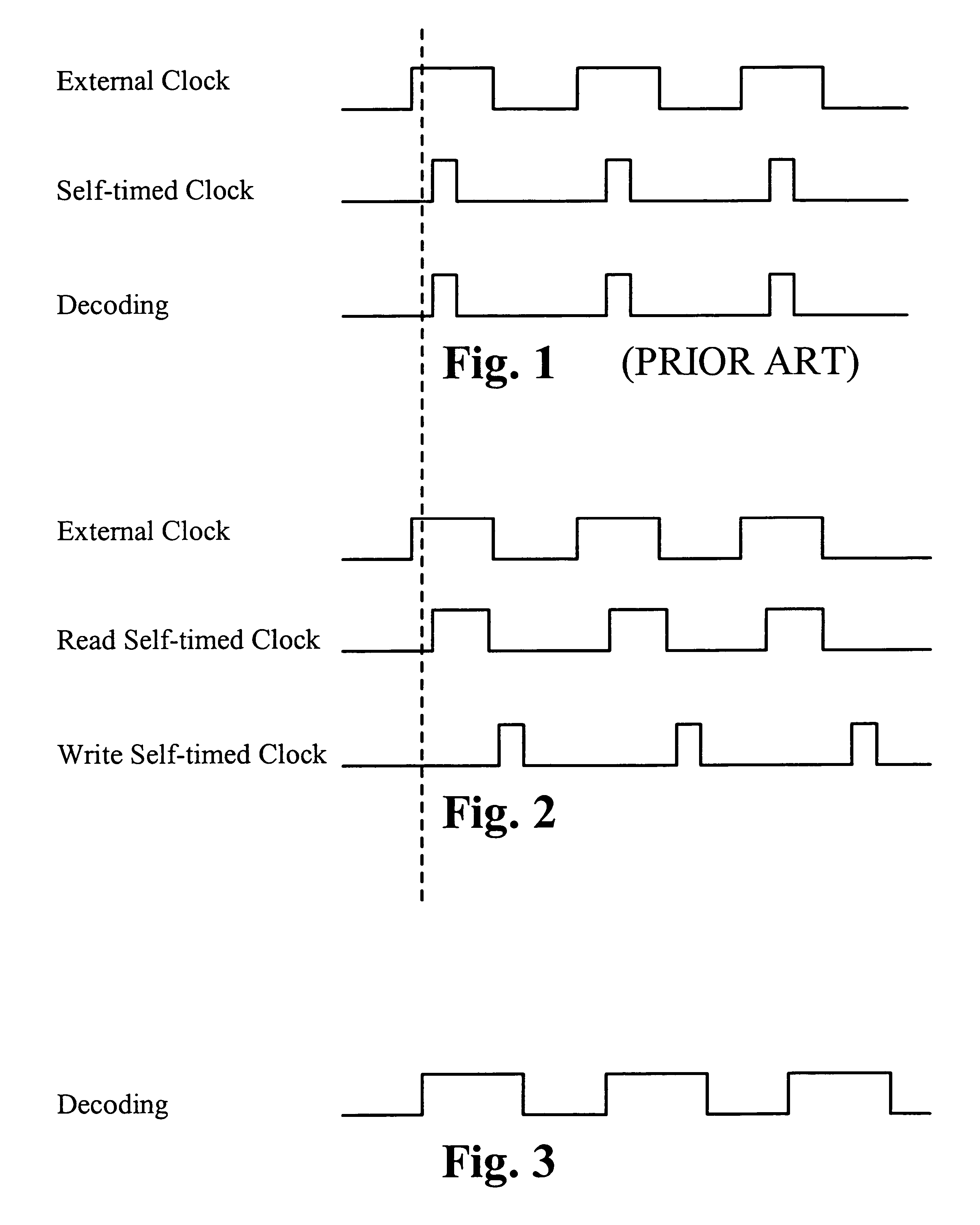
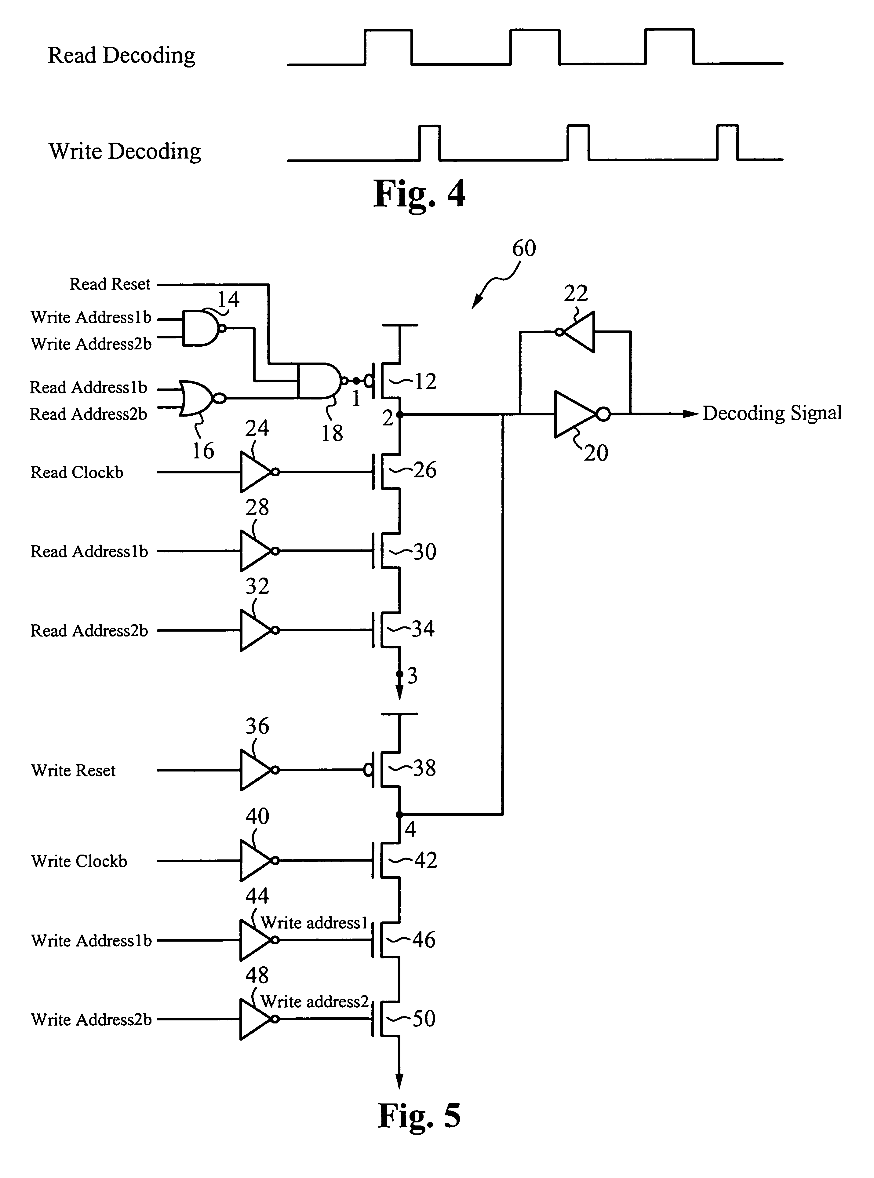
[0030]FIG. 2 illustrates the waveforms associated with the dual operation memory device. A clock generating circuit receives an external clock signal and generates a read self-timed clock signal and a write self-timed clock signal. The read self-timed clock signal includes a series of read self-timed pulses, each read pulse is triggered by a rising edge of the external clock signal. A read pulse width is determined by the time necessary to perform a corresponding read operation. The write self-timed clock signal includes a series of write self-timed pulses, each write pulse is triggered by a falling edge of a read pulse. A write pulse width is determined by a time necessary to perform a corresponding write operation. The clock generating circuit adds a gap time between each consecutive read pulse and write pulse to prevent write overlap. The read self-timed clock signal is used to subsequently generate a read decoding signal, where the read decoding signal corresponds to a read oper...


PUM


Abstract

A decoding signal circuit is configured to generate a dual operation decoding signal that enables a read operation and a write operation to be performed in one clock cycle. The decoding signal circuit is configured such that a read decoding signal and a write decoding signal are generated and multiplexed together to form the dual operation decoding signal. The memory device receives a read address and a write address consecutively in one cycle to generate the dual operation decoding signal. A single operation, such as a read only operation or a write only operation, can be performed as well as the dual operation of performing the read operation and the write operation in the same cycle.

Description

RELATED APPLICATIONS[0001]This application claims priority of U.S. provisional application, Ser. No. 60 / 731,395, filed Oct. 28, 2005, and entitled “DECODING FOR READ AND WRITE IN SAME CYCLE DUAL SELF-TIMED PULSE FOR READ AND WRITE OPERATION”, by the same inventors. This application incorporates U.S. provisional application, Ser. No. 60 / 731,395, filed Oct. 28, 2005, and entitled “DECODING FOR READ AND WRITE IN SAME CYCLE DUAL SELF-TIMED PULSE FOR READ AND WRITE OPERATION”, in its entirety by reference.FIELD OF THE INVENTION[0002]The present invention relates to the field of memory devices. More particularly, the present invention relates to the field of high-speed SRAM devices.BACKGROUND OF THE INVENTION[0003]Static Random Access Memory (SRAM) is a type of semiconductor memory. Data stored in an SRAM is retained as long as power remains applied, unlike dynamic RAM (DRAM) that needs to be periodically refreshed, read-only memory (ROM), or flash memory. SRAM is referred to as volatile ...

Claims


Application Information

Patent Timeline
Patent Type & Authority Patents(United States)
IPC IPC(8): G11C7/00
CPCG11C11/419
Inventor CHEN, HSIN-LEY SUZANNETSENG, CHIH-CHIANGHUANG, MU-HSIANG
Owner GSI TECH
Why Eureka
Try Eureka