Light emitting device having a layer of photonic crystals and a region of diffusing material and method for fabricating the device

a light emitting device and photonic crystal technology, which is applied in the direction of semiconductor devices, electrical devices, nanotechnology, etc., can solve the problems of reducing the overall led light output, and the inability of monochromatic leds to be used directly to produce broad-spectrum color light, so as to enhance the light output of the device

Inactive Publication Date: 2008-04-15
DOCUMENT SECURITY SYST
View PDF12 Cites 272 Cited by
  • Summary
  • Abstract
  • Description
  • Claims
  • Application Information

AI Technical Summary

Problems solved by technology

Due to the narrow-band emission characteristics, these monochromatic LEDs cannot be directly used to produce broad-spectrum color light.
A concern with conventional fluorescent LEDs is that a significant amount of light generated from a semiconductor die is lost due to reflection at the interface between the semiconductor die and the fluorescent encapsulant, which reduces the overall LED light output.
This reflection at the die / encapsulant interface is partly due to mismatch of indexes of refraction at the interface.

Method used


Image

  • Light emitting device having a layer of photonic crystals and a region of diffusing material and method for fabricating the device
  • Light emitting device having a layer of photonic crystals and a region of diffusing material and method for fabricating the device
  • Light emitting device having a layer of photonic crystals and a region of diffusing material and method for fabricating the device

Examples


Embodiment Construction

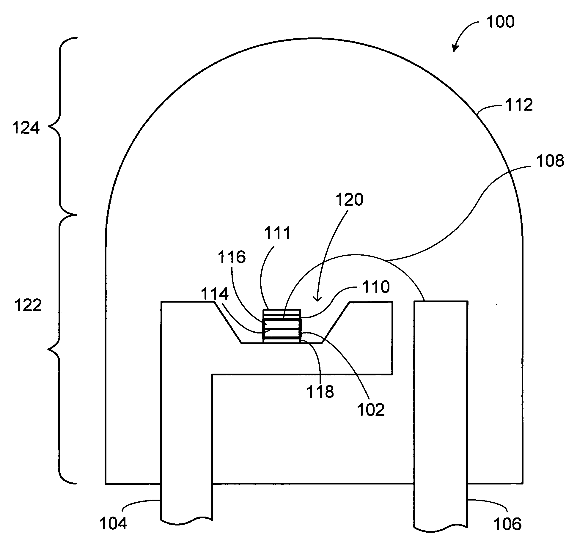
[0018]With reference to FIG. 1, a leadframe-mounted light emitting diode (LED) 100 in accordance with an embodiment of the invention is described. The LED 100 includes an LED die 102, leadframes 104 and 106, a bond wire 108, a layer 110 of three-dimensional (3-D) photonic crystals, a region of diffusing material 111 and an encapsulant 112. As described in more detail below, the photonic crystal layer 110 enhances light extraction from the LED die 102, which increases the light output of the LED 100, and the region of diffusing material 111 diffuses the light extracted from the LED die, which produces an output light having a uniform color.

[0019]The LED die 102 is a semiconductor chip that generates light of a particular peak wavelength. Thus, the LED die 102 is a light source of the LED 100. Although the LED 100 is shown in FIG. 1 as having only a single LED die, the LED may include multiple LED dies. The LED die 102 may be an ultraviolet LED die or a blue LED die. As an example, th...


PUM


Abstract

A light emitting device and method for fabricating the device utilizes a layer of photonic crystals and a region of diffusing material to enhance the light output of the device. The layer of photonic crystals is positioned over a light source, such as a light emitting diode die, and the region of diffusing material is positioned over the layer of photonic layer.

Description

BACKGROUND OF THE INVENTION[0001]Existing light emitting diodes (“LEDs”) can emit light in the ultraviolet (“UV”), visible or infrared (“IR”) wavelength range. These LEDs generally have narrow emission spectrum (approximately + / −10 nm). As an example, a blue InGaN LED may generate light with wavelength of 470 nm+ / −10 nm. As another example, a green InGaN LED may generate light with wavelength of 510 nm+ / −10 nm. As another example, a red AlInGaP LED may generate light with wavelength of 630 nm + / −10 nm.[0002]However, in some applications, it is desirable to use LEDs that can generate broader emission spectrums to produce desired color light, such as white light. Due to the narrow-band emission characteristics, these monochromatic LEDs cannot be directly used to produce broad-spectrum color light. Rather, the output light of a monochromatic LED must be mixed with other light of one or more different wavelengths to produce broad-spectrum color light. This can be achieved by introducing...

Claims


Application Information

Patent Timeline
Patent Type & Authority Patents(United States)
IPC IPC(8): H01L29/22H01L21/00H01L33/44
CPCB82Y10/00H01L33/44H01L33/508H01L2224/48091H01L2224/48247H01L2224/73265H01L2924/01077H01L2933/0083H01L2933/0091H01L2924/00014H01L2224/32245H01L2224/92247H01L2924/00H01L2924/12041H01L2924/00012
Inventor CHUA, JANET BEE YINLAU, YUE HOONG
Owner DOCUMENT SECURITY SYST
Why Eureka
Try Eureka