Asymmetrical memory cells and memories using the cells

a technology of memory cells and cells, applied in the field of electronic memory circuits, can solve the problems of affecting the stability of conventional sram during read mode, the stability of conventional sram is degraded with technology scaling, and the fluctuation of intra-device random mismatches among adjacent devices, so as to improve the read stability and improve the write performance and margin

Active Publication Date: 2008-04-22
GLOBALFOUNDRIES U S INC
View PDF8 Cites 55 Cited by
  • Summary
  • Abstract
  • Description
  • Claims
  • Application Information

AI Technical Summary

Benefits of technology

[0010]Principles of the present invention provide techniques for asymmetrical SRAM cells which can be improved, for example, by providing one or more of improved read stability and improved write performance and margin. In one exemplary embodiment, applicable to a variety of technologies, a memory cell for interconnection with true and complementary bit lines and read and write word lines includes a plurality of field effect transistors (FETS). The FETS form a first inverter and a second inverter cross-coupled to the first inverter. The first and second inverters are configured for selective coupling to the true and complementary bit lines under control of the read and write word lines. The first inverter is formed by first and second ones of the FETS, and the first FET is an n-type FET (NFET) and has an oxide layer with a thickness and a drive current. The second FET is a p-type FET (PFET) and has an oxide layer with a thickness.

Problems solved by technology

With shorter device channels and narrower widths, intrinsic device fluctuations and random mismatches among adjacent devices are significantly increased due to, e.g., random dopant fluctuations, short-channel effects, and narrow-width effects; thus, the stability of SRAM degrades with technology scaling.
The conventional SRAM has its worst stability during the READ mode because the voltage at the storage node having a “zero” logic value rises during the READ cycle.
If this increased node voltage is larger than the trip voltage of the inverter, the stored logic values will be flipped and data will be lost.
Thus, conventional symmetrical 6-T cells may be unstable when scaled to small sizes, and while the so-called asymmetrical SRAM cell can achieve an improved static noise margin (SNM) as compared to a conventional symmetrical SRAM cell, there are practical limits, due to device size considerations, to obtain further improvement in the SNM.

Method used


Image

  • Asymmetrical memory cells and memories using the cells
  • Asymmetrical memory cells and memories using the cells
  • Asymmetrical memory cells and memories using the cells

Examples


Embodiment Construction

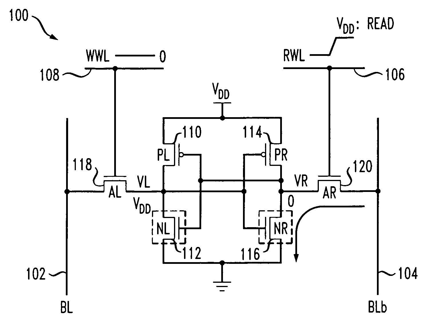
[0032]FIG. 1 depicts an asymmetrical SRAM cell not using techniques of the present invention. It will be appreciated that asymmetrical cell 100 can be part of a larger memory circuit having a plurality of bit line structures, such as those formed by true and complementary bit lines 102, 104. Such bit lines are also referred to as “BL” and “BLb.” Further, the circuit also includes a plurality of word line structures, such as those formed by read and write word lines 106, 108 (also referred to as “RWL” and “WWL” respectively) that intersect the plurality of bit line structures to form a plurality of cell locations. The cell 100 is asymmetrical, that is, there is not symmetry between the left and right portions of the cell 100.

[0033]The cell 100 can be selectively coupled to a corresponding one of the bit line structures formed by true and complementary bit lines 102, 104 under control of a corresponding one of the word line structures formed by read and write word lines 106, 108. Each...


PUM


Abstract

Techniques are provided for asymmetrical SRAM cells which can be improved, for example, by providing one or more of improved read stability and improved write performance and margin. A first inverter and a second inverter are cross-coupled and configured for selective coupling to true and complementary bit lines under control of read and write word lines. The first inverter is formed by a first, n-type, FET (NFET) and a second, p-type, FET (PFET). Process and / or technology approaches can be employed to adjust the relative strength of the FETS to obtain, for example, read margin, write margin, and / or write performance improvements.

Description

STATEMENT REGARDING FEDERALLY SPONSORED RESEARCH OR DEVELOPMENT[0001]This invention was made with Government support under contract number NBCH 3039004 awarded by the Defense Advanced Research Projects Agency (DARPA). The government has certain rights in this invention.FIELD OF THE INVENTION[0002]The present invention generally relates to electronic circuitry and, more particularly, to electronic memory circuits.BACKGROUND OF THE INVENTION[0003]Due to the increased portion of Static Random Access Memory (SRAM) arrays in the total chip area of modern chips, device dimensions in SRAM must be continuously scaled. With shorter device channels and narrower widths, intrinsic device fluctuations and random mismatches among adjacent devices are significantly increased due to, e.g., random dopant fluctuations, short-channel effects, and narrow-width effects; thus, the stability of SRAM degrades with technology scaling.[0004]The well-known conventional six transistor SRAM is described, e.g., ...

Claims


Application Information

Patent Timeline
Patent Type & Authority Patents(United States)
IPC IPC(8): G11C11/00
CPCG11C11/412H01L27/1104H10B10/12
Inventor CHUANG, CHING-TEKIM, JAE-JOONKIM, KEUNWOO
Owner GLOBALFOUNDRIES U S INC
Why Eureka
Try Eureka