RF amplifier with a bias boosting scheme

a technology of bias boosting and amplifier, which is applied in the direction of rf amplifier, high frequency amplifier, gain control, etc., can solve the problems of increasing the voltage drop of resistive components of the biasing circuit, increasing the difficulty of achieving sufficient control of the quiescent current, and adding additional resistors

Active Publication Date: 2008-04-29
MEDIATEK INC
View PDF8 Cites 45 Cited by
  • Summary
  • Abstract
  • Description
  • Claims
  • Application Information

AI Technical Summary

Benefits of technology

[0007]In accordance with another aspect of the present invention, the dc bias circuit includes a current source to provide bias current and an output terminal node coupled to a control terminal node of the power transistor via the first resistor.

Problems solved by technology

The continued increase in the average current also results in an increase in the voltage drop of resistive components of the biasing circuit.
Disadvantages of the cascode current mirror circuit and the modified Wilson current mirror circuit biasing schemes include the requirement of additional resistors to achieve accurate control of the quiescent current in the amplifying transistor due to a necessary isolation resistor between RF and biasing circuits.
Disadvantages of the stacked diode circuit with a capacitor include the greater difficulty of achieving sufficient control of the quiescent current since the stacked diode circuit does not form a current mirror circuit.

Method used


Image

  • RF amplifier with a bias boosting scheme
  • RF amplifier with a bias boosting scheme
  • RF amplifier with a bias boosting scheme

Examples


Embodiment Construction

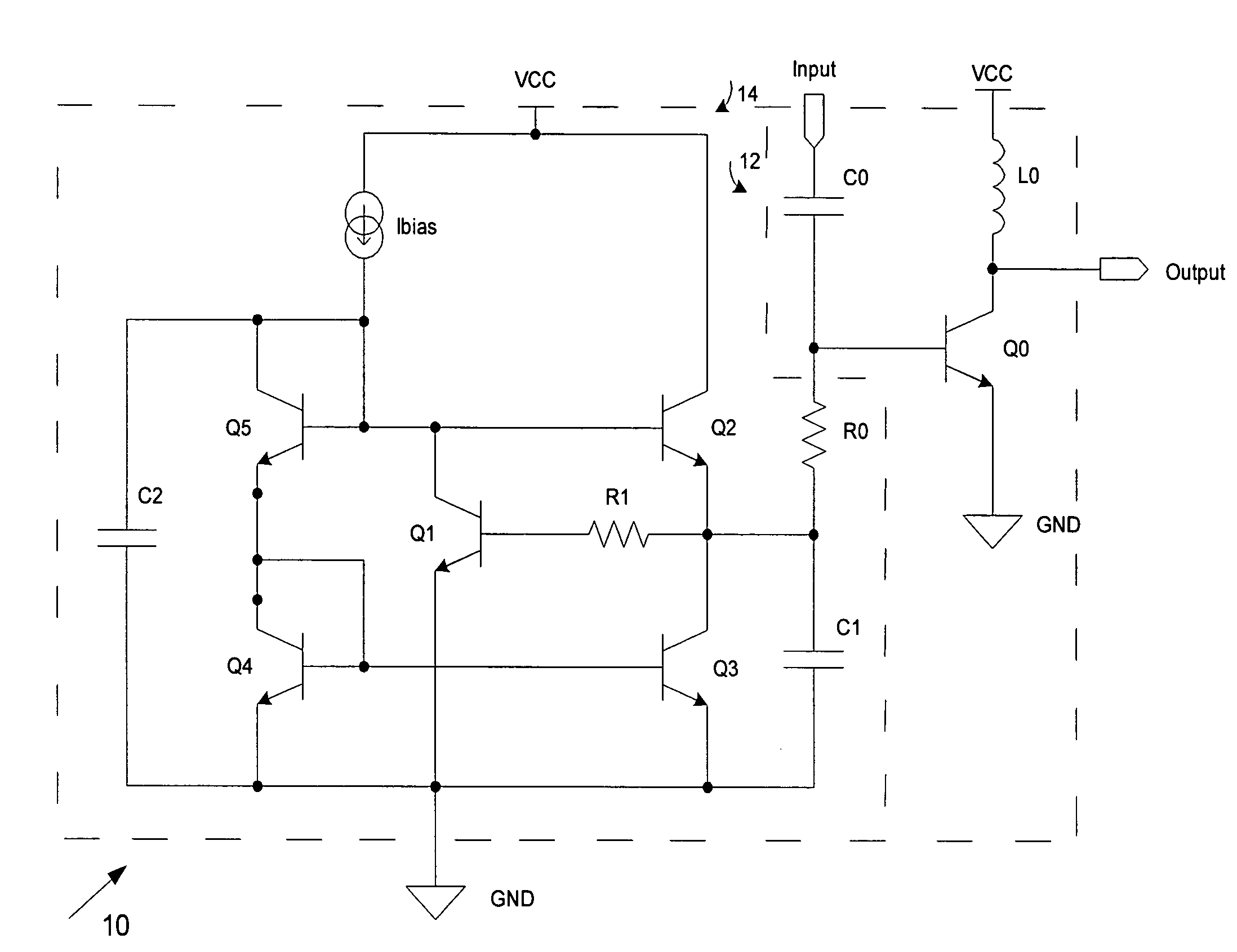
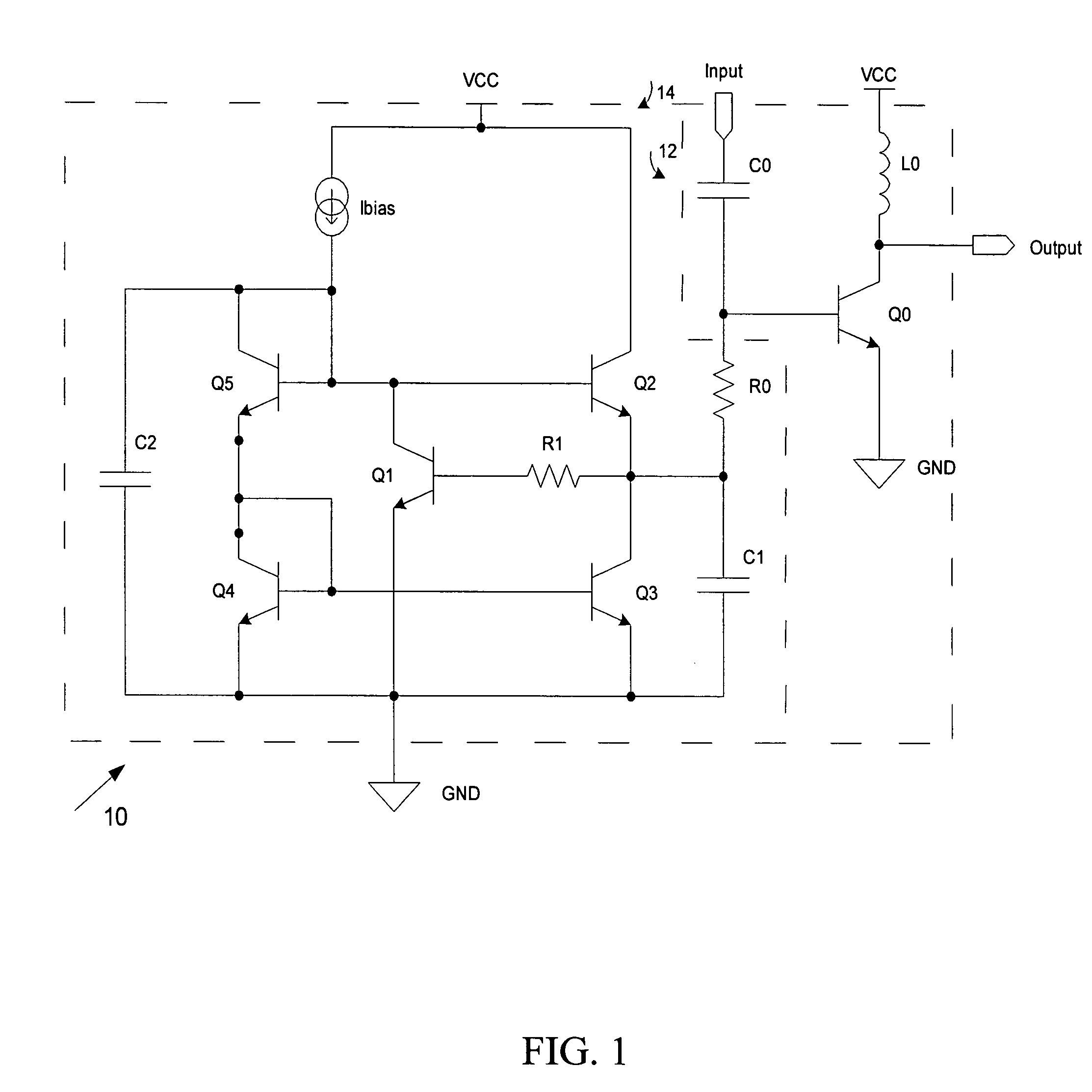
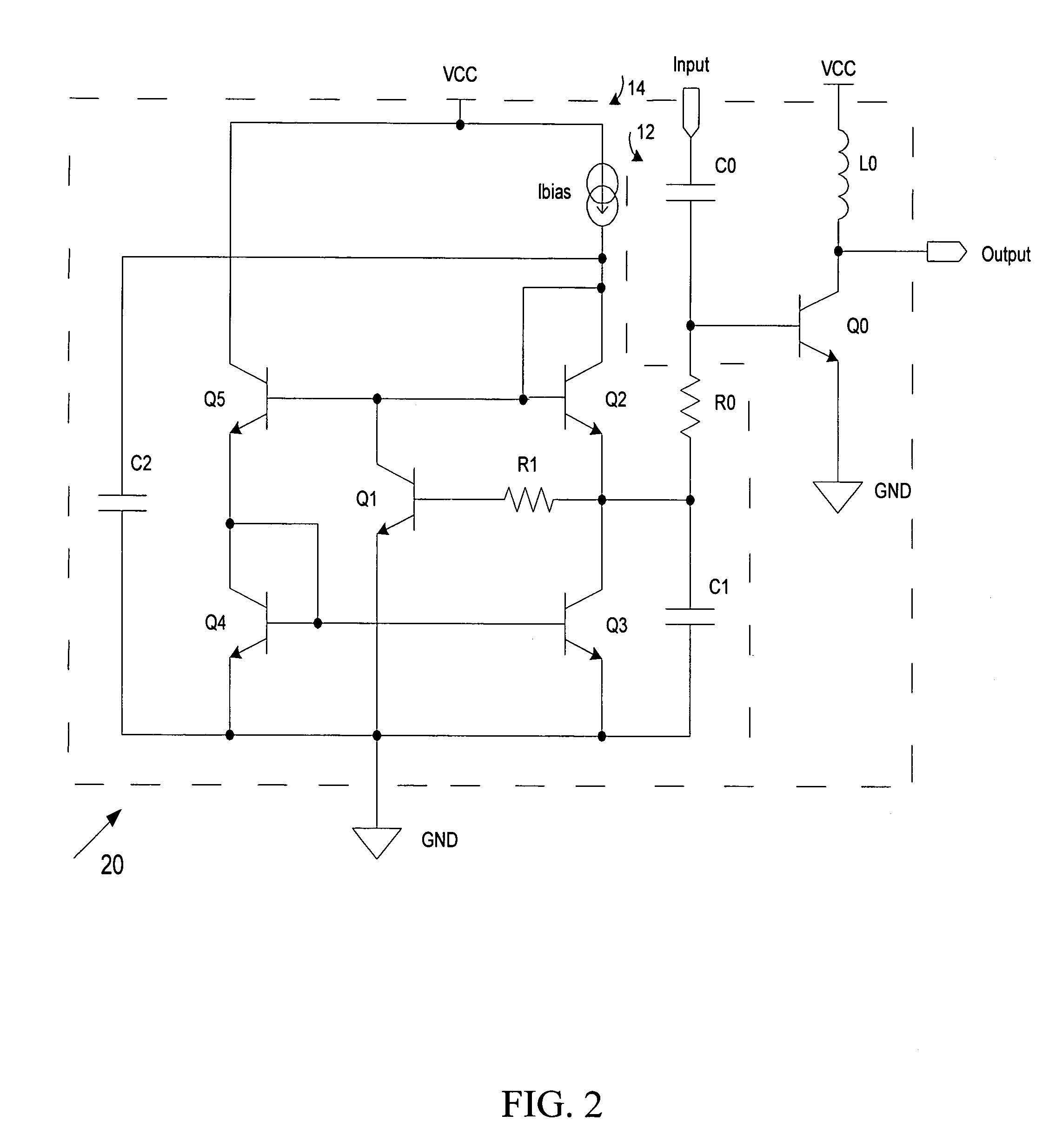
[0012]As disclosed below, the present invention provides methods and apparatuses for self-bias boosting of an output amplifying transistor circuit that comprise of modified current mirror circuits. In general, the present inventive RF amplifier apparatus comprises an amplifying transistor circuit and a dc bias circuit. In accordance to an embodiment of the present invention, the dc bias circuit comprises a dual current mirror with current gain to bias the output power transistor.

[0013]With reference to FIG. 1, a presently preferred embodiment of a power amplifier circuit 10 is shown. The inventive RF amplifier circuit generally comprises an amplifying transistor circuit 12 and a dc bias circuit 14. The dc bias circuit 14 comprises a modified current mirror, which acts as a self-bias boosting circuit for the amplifying transistor circuit 12. The modified current mirror provides a dual current mirror including a conventional current mirror and a cascode current mirror. Power transisto...


PUM


Abstract

The present invention provides methods and apparatuses for an amplifier circuit for amplifying an input signal. An amplifier circuit for amplifying an input signal comprises an amplifying transistor circuit having a power transistor and a dc bias circuit having a plurality of current mirror circuits and a discharge transistor wherein the discharge transistor and the power transistor form a combined current mirror circuit to control quiescent current in the power transistor.

Description

FIELD OF INVENTION[0001]The present invention relates to RF amplifiers for communication systems and, more particularly, to methods and apparatuses for bias boosting of the RF amplifier for communication systems.BACKGROUND[0002]RF amplifiers play a very important role in communication systems. A linear RF amplifier is usually biased for class AB operation to achieve higher power-added efficiency (PAE). In particular, RF amplifiers biased in a class AB mode are often used in high-frequency amplification. Typically, for a conventionally biased class AB amplifier, the average bias supply current increases as the RF input power increases. The continued increase in the average current also results in an increase in the voltage drop of resistive components of the biasing circuit. The increased voltage drop across the resistive components in turn reduces the average voltage drop across the forward biased PN junction of the amplifying transistor and pushes the amplifier into class B and pos...

Claims


Application Information

Patent Timeline
Patent Type & Authority Patents(United States)
IPC IPC(8): H03F3/04
CPCH03F1/30H03F3/189H03F2200/108H03F2200/18H03F2200/451
Inventor LUO, SIFENFAN, YIPINGLI, HONGYUCHAO, CHIEH-YUAN
Owner MEDIATEK INC
Why Eureka
Try Eureka