Display device

a technology of transistors and display devices, which is applied in the direction of static indicating devices, identification means, instruments, etc., can solve the problems of high power consumption, application of estimated degradation, etc., and achieve the effect of small variation in characteristic of driving tfts and low voltag

Active Publication Date: 2008-04-29
SEMICON ENERGY LAB CO LTD
View PDF25 Cites 28 Cited by
  • Summary
  • Abstract
  • Description
  • Claims
  • Application Information

AI Technical Summary

Benefits of technology

[0019]A high current capacity TFT is used as a driving TFT in a high gray-scale because it can supply a large current even with a lower Vgs, therefore, it does not operate in a linear region easily even when Vds is lowered. Therefore, luminance is not reduced when the EL element is degraded and operation with low voltage is possible. Thus, low power consumption and low heat generation can be realized, which prevents degradation of a TFT element.
[0020]A low current capacity TFT supplies current when high Vgs is applied. A low current capacity TFT is used for low gray-scale as a driving TFT because an effect of variation in characteristics of a TFT, in Vth particularly can be ameliorated by operating with a high Vgs. The use of this TFT is efficient particularly in the low gray-scale in which Vgs is low, and can enhance a display quality. Further, by designing a channel length L of the TFT long in order to suppress a current capacity, a variation in characteristics can be ameliorated.
[0026]According to the invention, by using a plurality of driving TFTs having different characteristics, an effect by the degradation of an EL element and variation in characteristic of the driving TFTs can be small and an operation at a low voltage is realized.

Problems solved by technology

However, a voltage with an estimated degradation has to be applied in advance, therefore, there are such problems as a high power consumption and heat generation caused by high voltage.

Method used


Image

  • Display device
  • Display device
  • Display device

Examples


embodiment mode 1

[0042]This application is based on Japanese Patent Application serial no. 2003-139665 filed in Japan Patent Office on 16 May, 2003, the contents of which are hereby incorporated by reference.

[0043]Although the present invention will be fully described by way of example with reference to the accompanying drawings, it is to be understood that various changes and modifications will be apparent to those skilled in the art. Therefore, unless otherwise such changes and modifications depart from the scope of the present invention, they should be construed as being included therein. Note that like components are denoted by like numerals in different drawings as of the configuration of the invention.

[0044]FIG. 4 shows an embodiment mode of the invention. A display device includes one or more of a pixel 406, and the pixel 406 comprises EL elements 402a and 402b respectively, driving TFTs 401a and 401b for driving the EL elements 402a and 402b, signal terminals 403a and 403b connected to gates...

embodiment mode 2

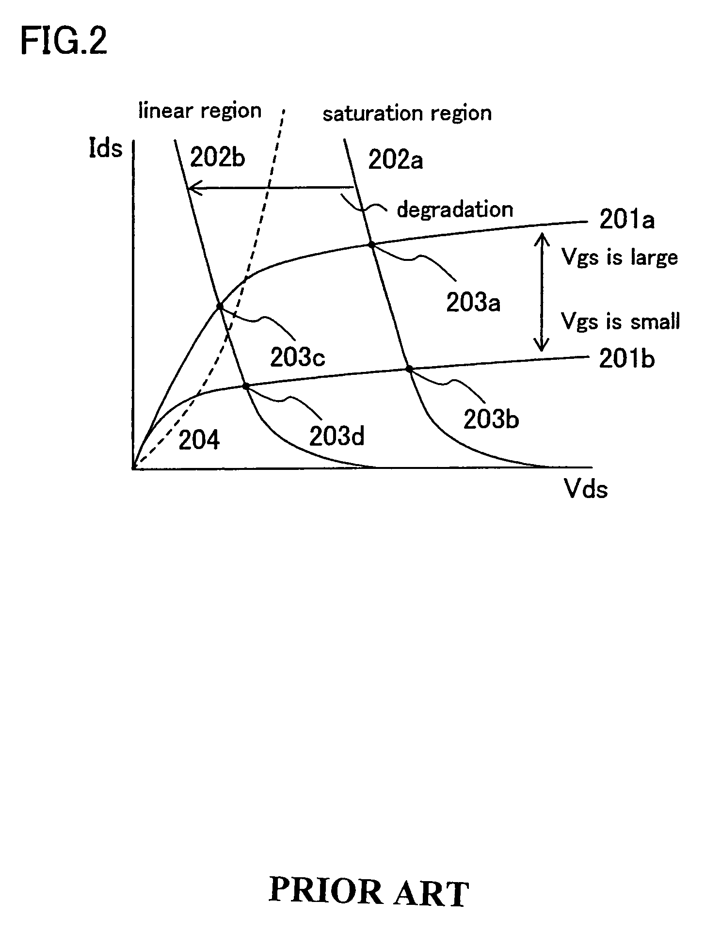
[0074]An embodiment mode of the invention is described with reference to FIGS. 8A and 8B. In order to set Vgs of the driving TFTs 401a and 401b at different voltages, a voltage of the driving TFT 401a is shifted in Embodiment Mode 1. A relation between Vgs of the driving TFT 401a and Vgs of the driving TFT 401b is shown in FIG. 8A. Here, Vgs of the driving TFT 401a is Vgsa and Vgs of the driving TFT 401b is Vgsb. When a characteristic line 811 shows the case of applying the same voltage as Vgsa and Vgsb, it corresponds to a characteristic line 812 in Embodiment Mode 1. In this embodiment mode, a different method for setting a voltage from Embodiment Mode 1 is described.

[0075]Vgsa is set so as to be low relatively to Vgsb in low gray-scale, while Vgsb is set so as to be close to Vgsa in higher gray-scale. A voltage setting in this embodiment mode is shown by a characteristic line 813.

[0076]FIG. 8B shows a Vgs-Ids characteristic line 801 a of the driving TFT 401a which is applied the ...

embodiment mode 3

[0079]An embodiment mode of the invention is described with reference to FIG. 9. Vgs of the driving TFTs 401a and 401b are set at different voltages in Embodiment Modes 1 and 2. In this embodiment mode, the driving TFT 401a can be mainly used in the high gray-scale and the driving TFT 401b can be mainly used in the low gray-scale even when Vgs of the driving TFTs 401a and 401b are the same.

[0080]It is assumed that a current supplied from the driving TFT 401a is Idsa and a current supplied from the driving TFTs 401b is Idsb. In this embodiment mode, a current that deducted a constant current Idiff from Idsa is supplied to the EL element 402a. A current Iel supplied to the EL elements 402a and 402b can be expressed by the following formula.

Iel=Idsa−Idiff+Idsb . . . (Idsa>Idiff) Iel=Ids . . . (Idsa≦Idiff)  [Formula 5]

[0081]FIG. 9 shows a Vgs-Ids characteristic line 901a of the driving TFT 401a which is applied Vgs, a characteristic line 901a′ that deducted Idiff from the characteristic...


PUM


Abstract

By operating a driving TFT in a saturation region, luminance is not easily reduced when an EL element is degraded. However, such problems occur as a high voltage, high power consumption, and heat generation. In the case of operating a driving TFT in a saturation region, luminance varies due to a variation of driving TFTs. In view of the aforementioned problems, a high current capacity TFT is used in the high gray-scale and a low current capacity TFT is used in the low gray-scale. The high current capacity TFT can supply a large current with a lower Vgs, therefore, it does not easily operate in a linear region even when Vds is lowered. Thus, a luminance is not reduced easily even when an EL element is degraded, and an operation at a low voltage is realized. The low current capacity TFT supplies current when high Vgs is applied. With high Vgs, an effect of variation in characteristics of TFTs, especially in Vth can be ameliorated.

Description

BACKGROUND OF THE INVENTION[0001]1. Field of the Invention[0002]The invention relates to a display device having a transistor. More specifically, the invention relates to a display device having an EL element and a thin film transistor (hereinafter referred to as a TFT) and the like formed on an insulator. Further, the invention relates to an electronic device having such a display device.[0003]2. Description of the Related Art[0004]In recent years, a display device having a light emitting element such as an electro luminescence (EL) element is actively developed. The light emitting element emits light by itself and does not use backlight which is required in a liquid crystal display (LCD) and the like, therefore, it is highly visible and suitable for fabricating in a thin form. Furthermore, its viewing angle is almost unlimited.[0005]Generally, an EL element emits light when a current is supplied. Therefore, a different pixel configuration from LCD is suggested (refer to Non-patent...

Claims


Application Information

Patent Timeline
Patent Type & Authority Patents(United States)
IPC IPC(8): G09G3/32G09G3/20H01L51/50G09F9/30G09F9/33G09G3/30H01L27/32H05B33/14
CPCG09G3/3233G09G3/3258G09G2300/0819G09G2300/0852G09G2300/0876G09G2310/0262G09G2320/043
Inventor MIYAGAWA, KEISUKE
Owner SEMICON ENERGY LAB CO LTD
Why Eureka
Try Eureka