Fingerprint input device

a technology of input device and fingerprint, which is applied in the direction of program control, instruments, testing/monitoring control systems, etc., can solve the problems of generating the reflectance product of the two reflectances, and achieve the effect of low cost and high practicality

Inactive Publication Date: 2008-04-29
NEC PERSONAL COMPUTERS LTD
View PDF21 Cites 82 Cited by
  • Summary
  • Abstract
  • Description
  • Claims
  • Application Information

AI Technical Summary

Benefits of technology

[0128]To irradiate light to the finger from the most directions, a surface light emission body is arranged around the fingerprint measured portion so that the emitted light is directed toward the finger and a shield is provided around the measured portion so that the light emitted from the surface light emission body does not directly enter the measured portion. The reason for using the surface light emission body is to make the light source surround the measured portion. To fulfill the same purpose, a so-called linear light emission body formed by linearly arranging, for example, light emission diode chips may be used in place of the surface light emission body. Such a linear light emission body has sufficient light amount and serves as a thin, efficient light source. Since a module of such a linear light emission body has been recently supplied at low cost as a light emission diode chip array, the linear light emission body is highly practical.

Problems solved by technology

As a result, in the fingerprint valley portion, reflectance is high on the two boundary surfaces and a reflection loss corresponding to the product of the two reflectances is generated when the scattered light from the finger is transmitted into the transparent solid film.

Method used


Image

  • Fingerprint input device
  • Fingerprint input device
  • Fingerprint input device

Examples


embodiment 1

[0160]FIGS. 12A and 12B show Embodiment 1 in which a very thin fingerprint input device according to the present invention is mounted on a printed circuit board. FIGS. 13, 14 and 15 show the operation states (operation principles) for fingerprint sensing when using the fingerprint input device, respectively.

[0161]FIG. 13 is a block diagram showing the configuration of the fingerprint input device according to Embodiment 1 of the present invention. In FIG. 13, reference numeral 5 denotes a two-dimensional image sensor which two-dimensionally detects the strength and weakness of light depending on the irregularities of a finger 1, 27 denotes an image processing portion which generates a fingerprint pattern by subjecting the output of the two-dimensional sensor 5 to an image processing, and 28 denotes a pattern recognition portion which extracts the feature of the fingerprint pattern generated by the image processing portion 27, compares the extracted feature with a predetermined refer...

embodiment 2

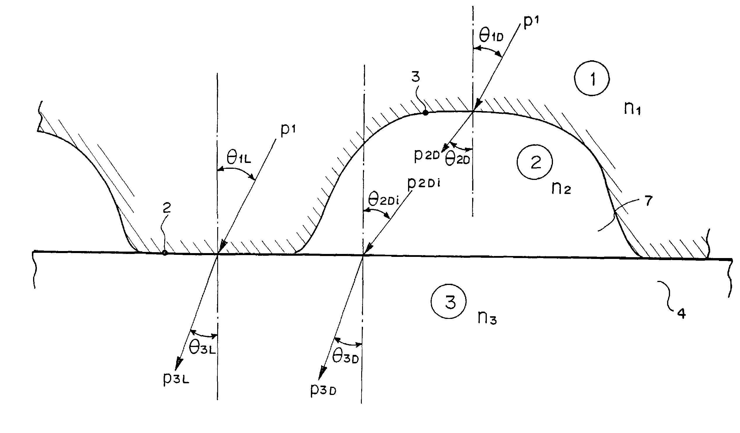
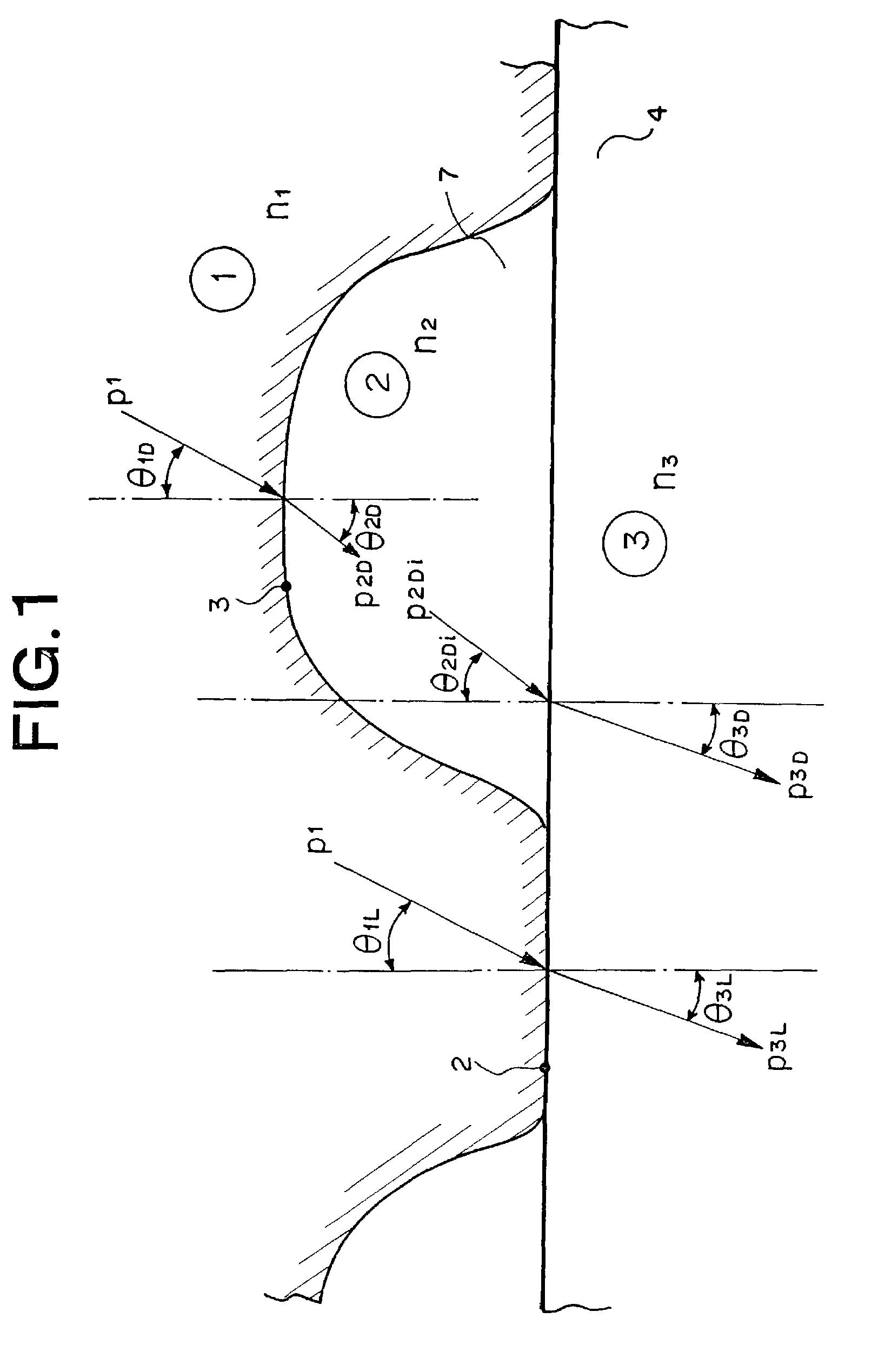
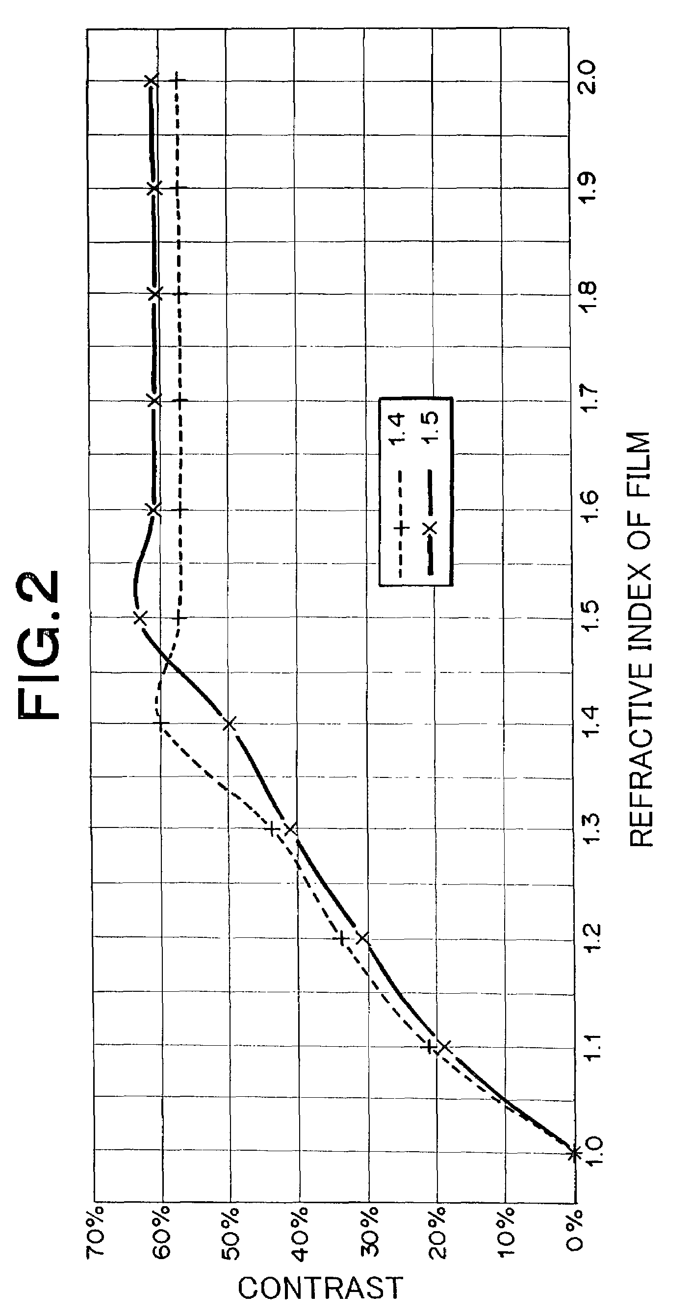
[0173]Embodiment 2 will next be described. FIGS. 16 and 17 are fragmentary sectional views of two kinds of fingerprint input devices according to Embodiment 2. A cover film 8 of a two-dimensional image sensor is intended to stabilize the characteristic of the sensor element, should be formed in a semiconductor manufacturing process and is normally thinner than several micrometers due to a semiconductor device manufacturing method used. If the finger is repeatedly, directly pressed against the cover film 8, the durability of the film 8 is adversely influenced by the contact of the finger. Therefore, in Embodiment 1, a transparent solid film 4 is provided and the thickness, refractive index and hardness of the transparent solid film 4 are specified. Among them, it is the thickness condition that contradicts the durability condition. Namely, as the transparent solid film 4 is thinner, a clearer image is obtained. As the transparent solid film 4 is thicker, the durability of the film im...

embodiment 3

[0186]In Embodiment 3, a micro-lens layer which has been recently used to enhance the sensitivity of an image sensor is employed as a protection film.

[0187]In Embodiment 3, a micro-lens 13 as a dome-shaped transparent solid is covered right over the photosensitive portion of an image sensor as shown in FIG. 20, whereby light incident on portions other than the photosensitive portion is converged on the photosensitive portion and the light detection sensitivity of the sensor is enhanced. When a fingerprint ridgeline portion contacts the micro-lens 13, the ridgeline is shaped as indicated by 13-1 and the light detection sensitivity of the sensor is enhanced by the convergence of the light on the photosensitive portion. However, the light incident on the micro-lens 13 from a valley portion 13-2 is emitted once to a space and the light from this portion becomes unavailable. As a result, the light in the 100% region of the fingerprint ridgeline portion cannot be detected. Nevertheless, s...


PUM


Abstract

A fingerprint input device capable of obtaining a fingerprint image presenting sufficient contrast is provided. The fingerprint input device includes: a two-dimensional image sensor for picking up a fingerprint image from a fingerprint measured portion of a measurement target finger; and a transparent solid film mounted on an image pickup surface of the two-dimensional image sensor, the fingerprint measured portion being mounted on the transparent solid film when the two-dimensional image sensor picks up the fingerprint image, wherein the fingerprint input device picks up an image of a fingerprint ridgeline portion in the fingerprint measured portion as a light portion, and picks up an image of a fingerprint valley portion in the fingerprint measured portion as a dark portion through an air layer, and a refractive index of the transparent solid film satisfies that contrast of the image is more than a given value.

Description

BACKGROUND OF THE INVENTION[0001]1. Field of the Invention[0002]The present invention relates to a fingerprint input device and particularly relates to a fingerprint input device for directly obtaining a fingerprint image using a two-dimensional image sensor.[0003]2. Description of Related Art[0004]Conventionally, a fingerprint input device of this type normally employs optical components such as a lens, a prism and an optical fiber, irradiates light to the fingerprint of a fingertip from a predetermined angle, converges light reflected by the fingerprint and outputs a fingerprint image. Further, a system of directly inputting a fingerprint image by electrostatic capacity instead of obtaining a fingerprint image using an optical system is studied.[0005]A system of directly inputting a fingerprint image by an optical device is also studied. As the system, there are known a light reflection system for irradiating light to a fingertip skin and using reflected light therefrom and a ligh...

Claims


Application Information

Patent Timeline
Patent Type & Authority Patents(United States)
IPC IPC(8): G06K9/00A61B5/117G06T1/00H01L27/14
CPCG06K9/00046A61B5/1172G06V40/1324G06F18/00
Inventor HIGUCHI, TERUYUKI
Owner NEC PERSONAL COMPUTERS LTD
Why Eureka
Try Eureka