Memory array with ultra-thin etched pillar surround gate access transistors and buried data/bit lines

a memory array and ultra-thin etching technology, applied in the direction of transistors, semiconductor devices, electrical apparatus, etc., can solve the problems of difficult formation of shallow junctions, difficult sub-threshold conduction, and significant problems in conventional transistor structures, so as to improve sub-threshold performance and improve the control of the conduction channel. , the effect of high device density

Active Publication Date: 2008-05-13
MICRON TECH INC
View PDF101 Cites 79 Cited by
  • Summary
  • Abstract
  • Description
  • Claims
  • Application Information

AI Technical Summary

Benefits of technology

[0012]Thus, various embodiments provide a memory array including access transistors over buried data / bit lines which include substantially surrounding gate structures which provide improved sub-threshold performance and relatively high device density. Certain embodiments provide the ability to fabricate relatively precisely defined device features of sub-photolithographic dimensions. Embodiments also provide word lines that contact surround gate structures for improved control of the conduction channel. These and other objects and advantages of the invention will be more apparent from the following description taken in conjunction with the accompanying drawings.

Problems solved by technology

Ongoing scaling of metal oxide semiconductor field effect transistor (MOSFET) technology to the deep sub-micron region where channel lengths are less than 0.1 micron (100 nanometers or 1,000 Å) causes significant problems in conventional transistor structures.
Such shallow junctions are difficult to form by conventional implantation and diffusion techniques.
Sub-threshold conduction is particularly problematic in dynamic random access memory (DRAM), as it significantly reduces the charge storage retention time of the capacitor cells.
Extremely high doping level generally results in increased leakage and reduced carrier mobility, thus making the channel shorter to improve performance is offset or negated by the lower carrier mobility and higher leakage.
This leakage current is a significant concern and problem in low voltage and low power battery operated complimentary metal oxide semiconductor (CMOS) circuits and systems, particularly in DRAMs.
This is shown in FIG. 2 as that if low voltages are used for this low power operation, then there is a problem with threshold voltages and standby leakage current being of large enough value to degrade overall circuit performance.

Method used


Image

  • Memory array with ultra-thin etched pillar surround gate access transistors and buried data/bit lines
  • Memory array with ultra-thin etched pillar surround gate access transistors and buried data/bit lines
  • Memory array with ultra-thin etched pillar surround gate access transistors and buried data/bit lines

Examples


Embodiment Construction

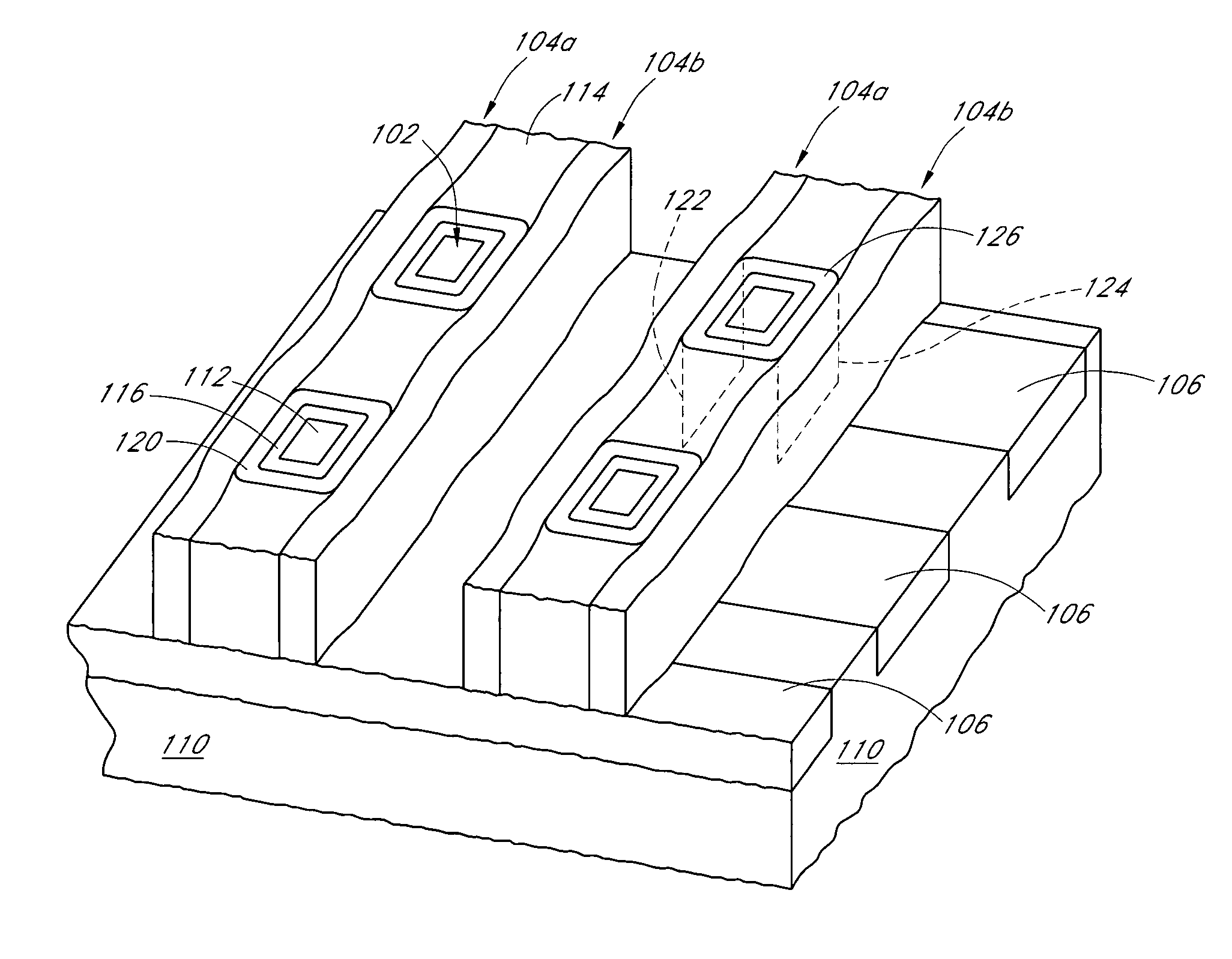
[0027]Reference will now be made to the drawings of the various embodiments of the invention wherein like reference numerals will refer to like parts / structures throughout. FIGS. 5A, 5B, and 6 illustrate a top section view, side section view, and perspective view respectively of one embodiment of a memory circuit access array 100, which in following will be referred to as the array 100 for brevity. The array 100 provides access with a plurality of memory cells, in certain embodiments an array of DRAM cells, which can be utilized for storage and access of information. The array100 comprises a plurality of access transistors 102, each of which is in electrical communication with a corresponding word line 104 and data / bit line 106. In this particular embodiment of the array 100, the word lines 104 are arranged generally parallel to each other. The data / bit lines are as well arranged substantially in parallel with each other, and also extending generally transversely with respect to the...


PUM


Abstract

A memory array with data/bit lines extending generally in a first direction formed in an upper surface of a substrate and access transistors extending generally upward and aligned generally atop a corresponding data/bit line. The access transistors have a pillar extending generally upward with a source region formed so as to be in electrical communication with the corresponding data/bit line and a drain region formed generally at an upper portion of the pillar and a surround gate structure substantially completely encompassing the pillar in lateral directions and extending substantially the entire vertical extent of the pillar and word lines extending generally in a second direction and in electrical contact with a corresponding surround gate structure at least a first surface thereof such that bias voltage applied to a given word line is communicated substantially uniformly in a laterally symmetric extent about the corresponding pillar via the surround gate structure.

Description

BACKGROUND OF THE INVENTION[0001]1. Field of the Invention[0002]The invention relates to the field of high density semiconductor memory arrays and more particularly to arrays with vertical transistors having sub-photolithographic device dimensions with ultra-thin pillars and substantially fully surrounding gates suitable for use as access transistors, such as for DRAM arrays.[0003]2. Description of the Related Art[0004]Ongoing scaling of metal oxide semiconductor field effect transistor (MOSFET) technology to the deep sub-micron region where channel lengths are less than 0.1 micron (100 nanometers or 1,000 Å) causes significant problems in conventional transistor structures. Generally, junction depth should be much less than the channel length, and thus for a channel length of, for example, 1,000 Å, this implies junction depths on the order of a few hundred Angstroms. Such shallow junctions are difficult to form by conventional implantation and diffusion techniques.[0005]FIG. 1 illu...

Claims


Application Information

Patent Timeline
Patent Type & Authority Patents(United States)
IPC IPC(8): H01L29/72
CPCH01L27/10876H01L27/10885H01L29/66666H01L29/7827H01L27/10891H10B12/053H10B12/488H10B12/482
Inventor FORBES, LEONARD
Owner MICRON TECH INC
Why Eureka
Try Eureka