Production method for electronic component and electronic component

a production method and electronic component technology, applied in the direction of printed circuit manufacturing, printed circuit components, printed element electric connection formation, etc., can solve the problems of reducing dimensional accuracy, unable to form wiring patterns of a narrow width, and unable to meet the requirements of electrical reliance, so as to improve electrical reliance and simplify steps

Active Publication Date: 2008-05-13
TDK CORPARATION
View PDF14 Cites 1 Cited by
  • Summary
  • Abstract
  • Description
  • Claims
  • Application Information

AI Technical Summary

Benefits of technology

[0022]In view of the above-noted problems peculiar to the prior art, the present invention has as its object to provide a method of manufacturing an electronic part in which electroless plating which is the ante-processing of electroplating, or other ante-processing corresponding thereto is disused to thereby make it possible to achieve the simplification of steps and also achieve an improvement in electrical reliance, and an electronic part.
[0031]Also, the present invention can cope with even a case where a circuit pattern is already formed on a lower layer and electric power supply cannot be effected from the lower layer side. Also, the edge portion of the electric power supplying portion is utilized and therefore, the precipitation speed of the plating layer is high and further, after the growth of the plating layer, the plating layer is precipitated with the aforementioned edge portion and the bottom surface of the opening portion as electrodes and therefore, it becomes possible to improve the precipitation speed of the plating layer.

Problems solved by technology

However, the use of the above-described electroless plating (and other method replacing the electroless plating) has posed such problems will be shown below.
When as shown in FIG. 10B, electroplating is effected to try to fill the opening portion 7 with a metal material after the electroless plating layer has been formed, the electroplating layer 9 is thickly formed on the whole of one side of the wiring layer and as the result, there has arisen the problem that when as shown in FIG. 10C, a wiring pattern is to be formed by etching, the cross section of this wiring pattern becomes trapezoid, and dimensional accuracy is reduced and a wiring pattern of a narrow width cannot be formed.
Also, in a case where electroless plating is not used, but other ante-processing is effected, there has been the possibility that a similar problem may arise.
However, if this metal catalyst is residual on the surface of a wiring layer, there has been the possibility that an insulation resistance value may be reduced or such trouble as the short-circuiting of a wiring pattern may be caused.
In the electronic parts in recent years, a narrower pitch has been advanced and the possibility of the occurrence of the above-noted trouble has more increased.

Method used


Image

  • Production method for electronic component and electronic component
  • Production method for electronic component and electronic component
  • Production method for electronic component and electronic component

Examples


Embodiment Construction

[0043]A method of manufacturing an electronic part according to the present invention, and an electronic part will hereinafter be described with respect to a preferred specific embodiment thereof shown in the drawings.

[0044]The electronic part according to the present embodiment is of a form in which wiring layers are successively laminated on the opposite sides of a core material. These laminated wiring layers are connected together to thereby form stereoscopic wiring structure.

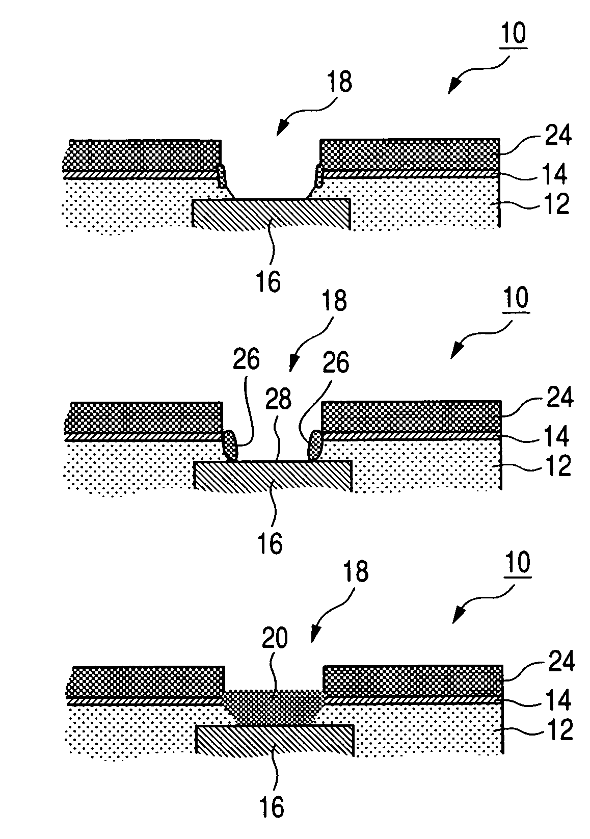
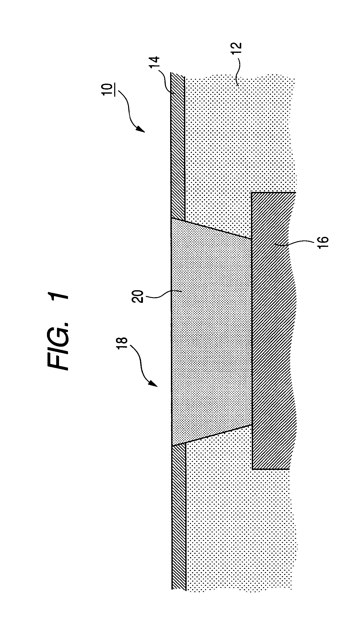
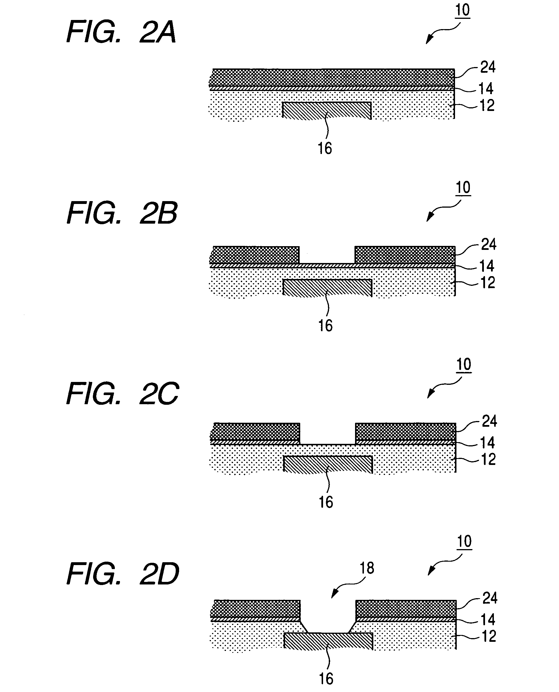
[0045]FIG. 1 is a cross-sectional view of essential portions showing a form immediately after a conductor portion has been formed in a wiring layer.

[0046]As shown in FIG. 1, the wiring layer 10 constituting an electronic part according to the present embodiment has a base member 12 comprising an insulating member having a predetermined thickness, copper foil 14 uniformly formed on the upper surface of this base member 12, and a columnar conductor 16 providing lower layer wiring formed in the interior of the ...


PUM


Abstract

A method of manufacturing an electronic part in which on the upper surface of an insulating member covering lower layer wiring, a conductor portion connected from the lower layer wiring is exposed. In this method, electric power supplying film is formed on the upper surface of the insulating member, whereafter an opening portion having the lower layer wiring as a bottom is formed from the electric power supplying film side. Then metal plating is grown from the edge portion of the electric power supplying film from the opening portion with the electric power supplying film as an electrode, and the opening portion is filled with the metal plating closely contacting with the lower layer wiring to thereby form a conductor portion.

Description

BACKGROUND OF THE INVENTION[0001]1. Field of the Invention[0002]This invention relates to a method of manufacturing an electronic part in which wiring layers are successively laminated on a core material, and an electronic part, and particularly to a method of manufacturing an electronic part which is suitable for forming an electrical conductor forming inter-layer connection in the wiring layers, and an electronic part.[0003]2. Related Background Art[0004]There is known an electronic part in which wiring layers are successively laminated on the surface of a core material, and connection is effected among these laminated wiring layers to thereby form stereoscopic wiring structure.[0005]In the wiring layers, there have been proposed and disclosed various manufacturing methods for forming a conductor portion forming inter-layer connection. FIGS. 8A to 8D of the accompanying drawings are process illustrations showing the conventional manufacturing process of the wiring layer of an elec...

Claims


Application Information

Patent Timeline
Patent Type & Authority Patents(United States)
IPC IPC(8): H01L21/302H05K3/42H05K3/40H05K3/46
CPCH05K3/423H05K3/421H05K3/4652H05K2201/09563H05K3/40
Inventor GOTOH, MASASHIKUWAJIMA, HAJIMEHARA, HIROKIYAMAMOTO, HIROSHI
Owner TDK CORPARATION
Why Eureka
Try Eureka