Unlock instant, AI-driven research and patent intelligence for your innovation.

Image processing apparatus and image processing program

a technology which is applied in the field of image processing apparatus and image processing program, can solve the problems of sensitivity variance between the pixels, false color or blurring of final produced color images, and variance in sensitivity between even pixels, so as to achieve high-accuracy interpolation and moderate the effect of sensitivity variation

Inactive Publication Date: 2008-05-13
OLYMPUS CORP
View PDF21 Cites 16 Cited by
  • Summary
  • Abstract
  • Description
  • Claims
  • Application Information

AI Technical Summary

Benefits of technology

The solution effectively mitigates the impact of sensitivity variations, producing higher-quality images by accurately interpolating missing color components and reducing the occurrence of grid patterns and other image distortions.

Problems solved by technology

This interpolation may cause the finally produced color images to undergo deterioration such as false color or blurring, unless ingenuity is exercised.
On the other hand, in an actual image pickup system, variance in sensitivity may occur between even pixels that use the same color filters and in fact should produce the same color components, due to a difference in gain between lines or slightly different spectral characteristics of the used color filters.
If the sensitivity differs at pixels where the same color components are obtained, however, this processing causes the sensitivity variance between the pixels to be directly reflected in the interpolation result.

Method used


Image

  • Image processing apparatus and image processing program
  • Image processing apparatus and image processing program
  • Image processing apparatus and image processing program

Examples


embodiment 1

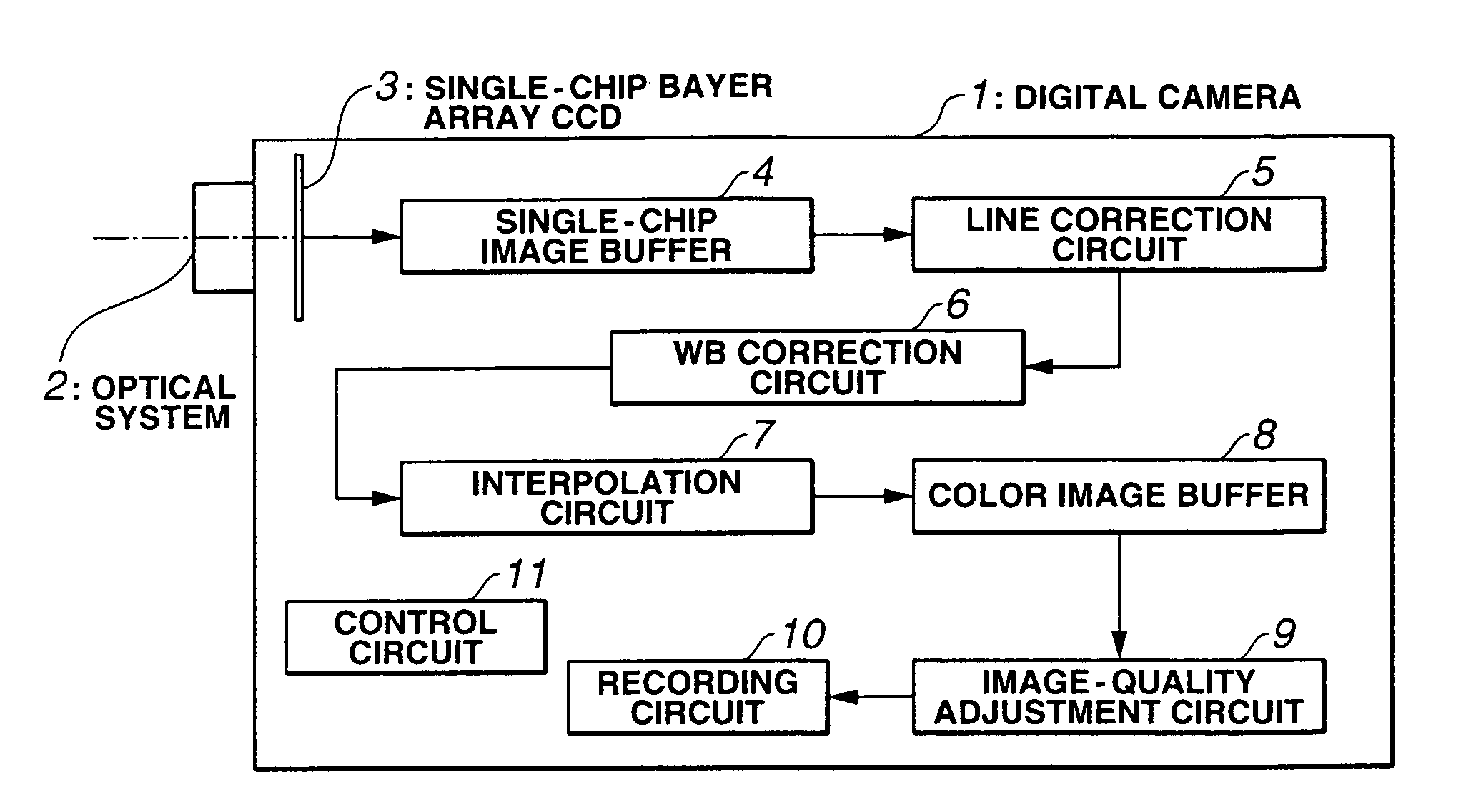
[0061]FIG. 1 shows Embodiment 1 according to the present invention. FIG. 1 is a block diagram showing the structure of a digital camera.

[0062]In this Embodiment 1, an image processing apparatus according to the present invention is applied to a digital camera.

[0063]As shown in FIG. 1, a digital camera 1 includes an optical system 2, a single-chip Bayer array CCD 3, a single-chip image buffer 4, a line correction circuit 5, a WB correction circuit 6, an interpolation circuit 7, a color image buffer 8, an image-quality adjustment circuit 9, a recording circuit 10, and a control circuit 11.

[0064]The optical system 2 is used to converge the luminous flux of an object.

[0065]The single-chip Bayer array CCD 3 applies photoelectric conversion to the image of the object focused by the optical system 2 and outputs an image pickup signal.

[0066]The single-chip image buffer 4 temporarily stores image data output from the single-chip Bayer array CCD 3 and then digitized by, for example, an A / D co...

embodiment 2

[0089]FIGS. 2 to 12 show Embodiment 2 according to the present invention. FIG. 2 is a block diagram showing the structure of a digital camera, FIG. 3 is a flowchart showing processing of a G-gap detection circuit, FIG. 4 is a diagram showing the classification of pixels in the G-gap detection circuit and the G interpolation circuit, FIG. 5 is a flowchart showing the processing by the G interpolation circuit, FIG. 6 is an illustration for the processing in step S16 of the processing by the G interpolation circuit shown in FIG. 5, FIGS. 7A to 7D are diagrams showing the direction in which weighting is calculated by a weighting-calculation circuit, FIG. 8 is a flowchart showing the processing by the RB interpolation circuit, FIGS. 9A and 9B are illustrations for the selection of pixels in step S31 of the processing by the RB interpolation circuit shown in FIG. 8, FIG. 10 is a flowchart showing the software processing carried out by a computer, FIG. 11 is a flowchart showing the G inter...

embodiment 3

[0177]FIGS. 13 to 16 show Embodiment 3 according to the present invention. FIG. 13 is a block diagram showing the structure of a digital camera, FIG. 14 is a diagram showing the numbers of pixels used for processing by the correction circuit, FIG. 15 is a flowchart showing processing by the correction circuit, FIG. 16 is a flowchart showing the software processing carried out by the computer.

[0178]In this Embodiment 3, the same components as those in the above-described Embodiments 1 and 2 are represented by the same reference numerals, and will not be described. The following description mainly focuses on the differences.

[0179]In this Embodiment 3, an image processing apparatus according to the present invention is applied to a digital camera as with Embodiment 1.

[0180]A digital camera 31 according to this Embodiment 3 is additionally provided with a correction circuit 32 as post-interpolation correcting means between the color image buffer 8 and the image-quality adjustment circui...


PUM


Abstract

The present invention is an image processing apparatus applied to a digital camera which includes a Bayer array CCD for producing and outputting an image lacking at least one type of color component per pixel by capturing an optical image focused by an optical system, a line correction circuit for correcting the difference in gain between lines on the image output from the CCD via a single-chip image buffer, and an interpolation circuit for producing color image data by interpolating a missing color component at each pixel of the single-chip image data output from the line correction circuit via a WB correction circuit based on information regarding neighborhood pixels.

Description

[0001]This application claims benefit of Japanese Application No. 2003-161185 filed in Japan on Jun. 5, 2003, Japanese Application No. 2004-155244 filed in Japan on May 25, 2004, Japanese Application No. 2004-158924 filed in Japan on May 28, 2004, the contents of which are incorporated by this reference.BACKGROUND OF THE INVENTION[0002]1. Field of the Invention[0003]The present invention relates to image processing apparatuses and image processing programs for processing images output from a single-chip image pickup system, a two-chip image pickup system, or a three-chip pixel-shifting image pickup system to generate a color digital image with three color component values at each pixel.[0004]2. Description of the Related Art[0005]Single-chip image pickup systems frequently used in, for example, digital cameras use a single-chip image pickup element having a different color filter for each pixel, and an image output from the image pickup element has only one type of color component v...

Claims


Application Information

Patent Timeline
Patent Type & Authority Patents(United States)
IPC IPC(8): G06K9/32G06K9/40G06K9/00H04N23/12G06T3/40H04N23/13
CPCG06T3/4015H04N9/045H04N2209/046H04N23/843H04N25/134
Inventor TSUKIOKA, TAKETO
Owner OLYMPUS CORP
Features
  • R&D
  • Intellectual Property
  • Life Sciences
  • Materials
  • Tech Scout
  • Unparalleled Data Quality
  • Higher Quality Content
  • 60% Fewer Hallucinations
Learn More