Unlock instant, AI-driven research and patent intelligence for your innovation.

Semiconductor memory device and method for reading semiconductor memory device

a memory device and semiconductor technology, applied in the field of semiconductor memory devices, can solve the problems of long cycle time, slow deactivation of memory cell mc word line wl, delay in pre-charge start time, etc., and achieve the effect of shortening the cycle time for reading

Inactive Publication Date: 2008-05-20
SONY CORP
View PDF7 Cites 6 Cited by
  • Summary
  • Abstract
  • Description
  • Claims
  • Application Information

AI Technical Summary

Benefits of technology

The present invention provides a semiconductor memory device that can generate a timing signal by a dummy memory cell, which can shorten the cycle time for reading data without depending upon the precharge time of the dummy bit line. This can reduce power consumption and improve the efficiency of the memory device. Additionally, the invention provides a method for precharging the first and second bit lines to a predetermined potential to discharge them and detect the voltage difference between them, which can further improve the speed of reading data from the memory cells.

Problems solved by technology

In the above reading method, however, after the internal timing control circuit 18b receives the timing signal S14 via the timing signal line TL, the dummy bit lines DBL and xDBL, connected to the dummy memory cell DMC, are precharged; therefore, a start time of the precharge is delayed, so there is a problem of a long cycle time.
Further, the deactivation of the word line WL of the memory cell MC is slow.
Therefore, the bit lines BL and xBL of the memory cell MC repeat a precharge and discharge operation in each cycle from a (voltage) power source Vcc to a reference voltage GND, so there is a problem that excessive power is consumed.
As a result, the transmission characteristics of the signal, particularly the rise and fall (time) of the pulse waveform become slow.
Namely, a delay occurs due to the distance of the signal line, so there is a problem of a long cycle time.

Method used


Image

  • Semiconductor memory device and method for reading semiconductor memory device
  • Semiconductor memory device and method for reading semiconductor memory device
  • Semiconductor memory device and method for reading semiconductor memory device

Examples


first embodiment

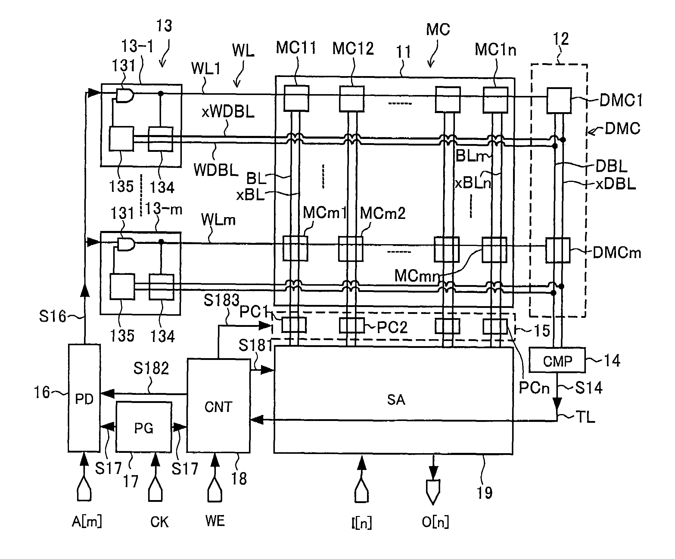
[0037]FIG. 1 is a block diagram showing a semiconductor memory device according to the present invention. A semiconductor memory device 1 according to the present embodiment has a dummy memory cell. When reading the data from the memory cell, it determines the timing of the reading of the data in accordance with the level (also referred to as the potential) of the dummy bit line connected to the dummy memory cell.

[0038]In more detail, based on the timing signal output when the voltage difference of the dummy bit lines connected to the dummy memory cell becomes the previously set threshold voltage at the time of the discharge, the read timing of the data from the memory cell is controlled, then the activation time of the word line and the timing start time of the precharge of the dummy bit lines to which the dummy cell is connected to the predetermined potential are controlled.

[0039]The semiconductor memory device 1 according to the present embodiment has, for example, as shown in FI...

second embodiment

[0106]FIG. 7 is a block diagram showing the semiconductor memory device according to the present invention.

[0107]A semiconductor memory device 1a according to the present embodiment has substantially the same configuration as that of the semiconductor memory device 1 according to the first embodiment, so the same components are assigned the same notations and the explanations thereof will be omitted. Only the difference will be explained.

[0108]The difference between the first embodiment and the second embodiment resides in the point that a word line driver 13 for the dummy memory cell 12 and a word line 13a for the memory cell 11 are separately provided.

[0109]The word line driver 13 for the dummy memory cell 12a of the semiconductor memory device 1a shown in FIG. 7 is substantially the same as the word line driver 13 shown in FIG. 4. The word line WL may be read as the dummy word line DWL.

[0110]FIG. 8 is a functional block diagram of the word line driver 13a of the semiconductor mem...


PUM


Abstract

A semiconductor memory device having a dummy memory cell and a reading method of the same, wherein provision is made of a memory cell 11 connected to a word line WL and a pair of bit lines BL and xBL, a dummy memory cell 12 connected to a word line WL and a pair of dummy bit lines DBL and xDBL, and a word line driver 13 for activating the word line at a common timing, and when the data is read out from the memory cell, a timing of the reading of the data is determined in accordance with a level of the dummy bit lines connected to the dummy memory, and when a voltage difference of a pair of dummy bit lines becomes a threshold voltage, the word line driver deactivates the word line and precharges the dummy bit lines.

Description

TECHNICAL FIELD[0001]The present invention relates to a semiconductor memory device for reading data of a memory cell based on a timing signal of, for example, a dummy memory cell and a method for reading the semiconductor memory device.BACKGROUND ART[0002]A semiconductor memory such as an SRAM (static random access memory) or ROM (read only memory), having a dummy memory cell and reading the data of a memory cell based on the timing signal of the dummy memory cell, is known.[0003]FIG. 11 is a functional block diagram of a semiconductor memory device provided with a general dummy memory cell. FIGS. 12A to 12G are timing charts of the semiconductor memory device shown in FIG. 11. A simple explanation will be given on a read operation of a SRAM, ROM, or other semiconductor memory device provided with a general dummy memory cell DMC with reference to FIG. 11 and FIGS. 12A to 12G.[0004]A signal S182b is output to a predecoder 16 by an internal timing control circuit 18b. When a predeter...

Claims


Application Information

Patent Timeline
Patent Type & Authority Patents(United States)
IPC IPC(8): G11C7/00G11C11/41G11C11/419
CPCG11C11/419G11C11/416
Inventor TOKITO, SHUNSAKU
Owner SONY CORP
Features
  • R&D
  • Intellectual Property
  • Life Sciences
  • Materials
  • Tech Scout
  • Unparalleled Data Quality
  • Higher Quality Content
  • 60% Fewer Hallucinations
Learn More