Optical amplification in photonic switched crossconnect systems

Active Publication Date: 2008-05-27
CALIENT TECH
50 Cites 2 Cited by

AI-Extracted Technical Summary

Problems solved by technology

With these transmission rates, however, has come a bottle neck in the central office where switching is performed to transmit information arriving over one optical fiber onto another optical fiber and toward the desired location.
Unfortunately, however, such switching is dependent upon the particular protocol within which the data is encoded, and is extremely expensive, complex and physically large in high data rate implementations, for example forty gigabits per second.
Of course, significant electrical power is consumed, and the solution does not scale to changes in data rate, port density or protocol.
One disadvantage of all of the systems described above is the inherent lo...

Method used

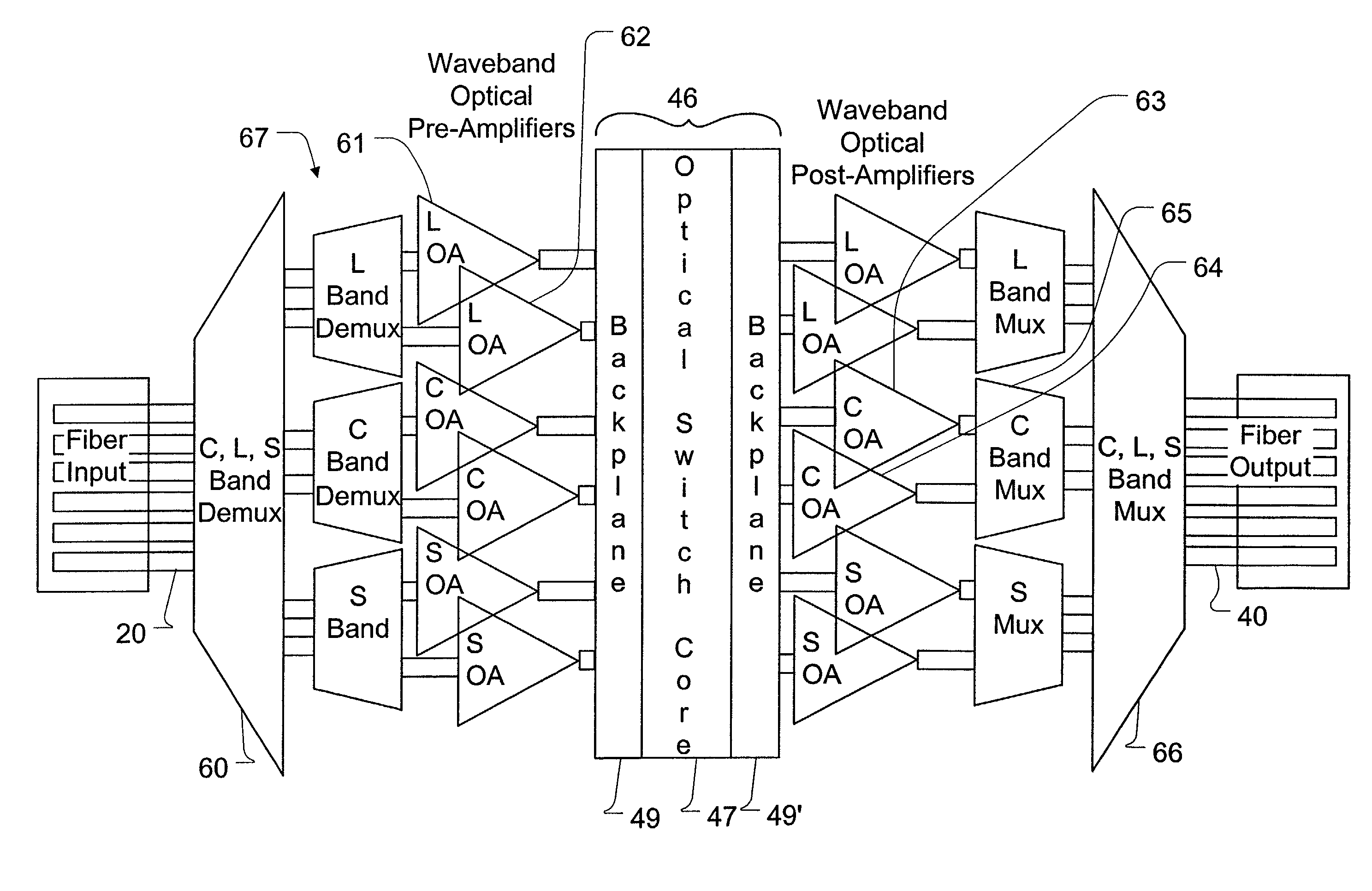
[0036]This invention relates to the provision of optical amplification within a MEMS switch. Present MEMS switches, such as the Calient DiamondWave™ photonic switch, do not include optical amplification. Thus, there is some loss in signal during the switching process. By providing optical amplification, a no-loss switch, or an amplified switch, is provided. This facilitates overcoming a number of problematic applications, such as increasing the size of a PXC switch beyond 1,000 by 1,000 (a size at which losses become significant), allowing a PXC switch to act as an active or passive wavelength equalizer or regenerator, boosting output power to a desired level to allow easier scaling and design of all-optical networks, etc.
[0045]Continuing now with the discussion of amplification, a known output power sense circuit 89 measures the output power of the signal at node 86 at the out put of the PXC 75. The output of circuit 89 is also provided to circuit 85 for the purposes of determining, from a comparison of signal strength at the input and output sides of the PXC 75, the extent, if any, of power correction required to account for power loss attributable to PXC 75. The control system shown in FIG. 7 allows balancing PXC and interface card losses with gain to assure overall improved operation of the system.
[0049]FIG. 10 is a diagram similar to FIG. 6. FIG. 10, however, illustrates an embodiment of the invention in which the input interfaces and the output interfaces each have amplification. (In the embodiment of FIG. 6 only the input side was amplified.) The elements depicted in FIG. 10 have been given corresponding reference numerals to those in FIG. 6, except that the output interfaces are now designated to reflect their inclusion of output optical amplifiers 78. For the embodiment depicted in FIG. 10, the input amplifiers 72 are used to boost the input signal's dynamic range with a fixed gain to compensate, for example, for switch losses. In a manner similar to that described with respect to FIG. 7, a series of taps and monitors are provided to detect the power levels an...

Benefits of technology

[0015]Another advantage of the invention is that the gain control may be done within a node and across multiple nodes via fiber optical links using control plane software. Typical control plane software can be generalized multiprotocol label switching (GMPLS). Using this kind of control, the amplifier gain can be used to equalize losses across an arbitrary number of switches and network elements based on power sensed at any point within the network
[0016]This invention provides an improved photonic switch in which optical amplification is provided for the signals before they are switched, after they are switched, or both before and after they are switched. The optical amplification compensates for fixed losses within the switch and transmission system, or provides output power equalization enabling the optical signals emerging from the photonic switch to have equal (or predetermined) power levels on a signal-by-signal (pre mux) basis.
[0017]Preferably, the photonic switching system includes a demultiplexer which is connected to a set of optical fibers. The demultiplexer separates a WDM optical signal into its constituent signals, placing each on its own optical fiber, and supplies those optical signals separately from each other to optical amplifiers. Typically, the amplifiers are provided on a per-wavelength or per-waveband basis. ...

Abstract

An improved photonic switch having optical amplification is described. Signals are amplified before they are switched, after they are switched, or both before and after they are switched. The optical amplification compensates for fixed losses within the switch and transmission system, or provides output power equalization. The photonic switching system includes a demultiplexer for dividing incoming light into different wavelengths or wavebands. The different signals are then supplied to optical amplifiers. The amplifiers amplify the optical signals before supplying them to the optical switch core. Once in the optical switch core, the signals are switched as desired to specified output nodes, then multiplexed back together to provide an output signal from the photonic switching system. In some systems amplification is further provided on the output side. The system also provides a control system by which the optical power of the signals is sensed and controllably amplified to achieve desired results, for example, fixed loss compensation, output power equalization, or other desired levels.

Application Domain

Multiplex system selection arrangementsWavelength-division multiplex systems +2

Technology Topic

Cross connectionOptical power +11

Image

  • Optical amplification in photonic switched crossconnect systems
  • Optical amplification in photonic switched crossconnect systems
  • Optical amplification in photonic switched crossconnect systems

Examples

  • Experimental program(1)

Example

[0037]FIG. 3 illustrates a first embodiment of the invention in which optical amplification is performed between demultiplexer 45 and PXC 46. As shown in FIG. 3, the optical fiber or fibers 20 are supplied to the wavelength division demultiplexer 45, and then through single channel (single wavelength) optical amplifiers (commonly known as amplets) 48. Amplets 48 may, for example, comprise known erbium doped fiber amplifiers, waveguide amplifiers, semiconductor optical amplifiers, and other appropriate optical amplifier technologies. These optical preamplifiers amplify the optical signals before they are provided to the input back plane 49, optical switch core 47, and output back plane 49′ and then switched out onto other optical fibers. If desired, a bank of multichannel optical post amplifiers 50 with (or without) equalization can be provided at the output of PXC 46. Alternatively, amplifiers may be provided only on the output side of PXC 46. After the post amplifiers 50, another wavelength multiplexer 51 returns the multiplexed signals to the output fiber bundle 40. In FIG. 3, the optical amplifiers are provided within the input and output interfaces of the optical switch, and may be individually controlled, so that they can be used to manage power levels, compensate for losses, and equalize loss nonuniformities which are a function of wavelength or other parameters, and other applications on a signal-by-signal basis. This allows amplification based on the selection of line cards, enabling each switch to be customized to the needs of the customer or location, without impacting the design of the optical switch core 47 itself. Thus, the apparatus of FIG. 3 provides optical amplification at the input and/or output interfaces on a waveband basis. A waveband is a collection (group) of wavelengths that are kept together throughout the transmission, switching and amplification process.
[0038]In contrast, FIG. 4 illustrates the provision of optical amplification at the switch input and/or output interfaces on a waveband basis. As shown in FIG. 4, the fibers provide signals to, and receive signals from, the same apparatus. In FIG. 4, however, rather than provide a separate amplifier for each wavelength, the wavelengths are grouped into “bands” with each band being amplified separately. As shown, optical amplifiers 52 and 54 provide amplification on groups of wavelengths as necessary. The optical amplifiers may, for example, comprise known erbium doped fiber optic amplifiers. While the approach of FIG. 4 does not allow tuning of the amplification to as fine a degree or resolution as FIG. 3, that is, on a wavelength by wavelength basis, it does provide amplification largely where it is needed most, that is, on a group of wavelengths, i.e., a waveband. It also reduces the number of amplifiers, and hence the cost, required to configure PXC 46.
[0039]FIG. 5 is a schematic diagram illustrating how waveband multiplexing may be combined with specific amplification of particular wavebands to provide overall optical amplification in an optical switch. Because optical amplifier technologies are often more cost effective (or technologically feasible) when used to amplify specific regions (wavebands) of the optical spectrum, this is important. Instead of using one very expensive or complex amplifier to boost all wavelengths, this technique separates out wavebands first and then directs these wavebands to the appropriate optical amplifier. As shown, the fiber bundle 20 is provided to a band demultiplexer 60. Demultiplexer 60 demultiplexes the incoming optical signals into L, C, and S-bands. In a preferred embodiment, the C-band is the conventional waveband extending from 1528.77 to about 1563.04 nm. The L-band is the long wavelength band, extending from about 1570.42 to 1603.17 nm. The S-band is the short wavelength band, and extends from about 1520 to 1535 nm. Each of the wavebands may then be further demultiplexed, if desired, by a second stage of demultiplexers 67. By demultiplexing in this manner, future changes in technology with respect to transmitted wavelengths can be accommodated, yet amplification can be provided with respect to the specific needs of the frequency band of interest.
[0040]As shown in FIG. 5 the further demultiplexed L-band signals are provided to two (or more) optical preamplifiers 61 and 62. Similar demultiplexed signals on the C-band and the S-band are provided to the corresponding optical preamplifiers, as well. All of the optical preamplifiers are coupled to the back plane 49 of PXC 46. After switching, if desired, optical post amplifiers can be applied to the signals in the same manner. For example, waveband post-amplifiers 63 and 64 are shown receiving signals from back plane 49′ and providing them to a C-band multiplexer 65. Once the C, L and S-bands are individually multiplexed, all three bands may be multiplexed together by multiplexer 66, to place output signals on fiber bundle 40. Of course, other known multiplexing arrangements may also be used.
[0041]The preceding has been a description of the overall system architecture of the invention as it applies to providing optical amplification in PXC switches. The system provided is scaleable, can be configured for different optical wavebands as new technologies appear, compensates for loss in the optical switch, and provides for equalizing (or individually adjusting) channel power at the switch output so that each signal is of relatively the same (or a desired) magnitude. Finally, the system also provides a technique for assuring that a specified output power level is provided at each channel, which power level is independent of the power level of the input signal or the power level of other constituent signals in the multiplexed signal.
[0042]FIG. 6 is a schematic diagram which illustrates the optical amplifiers located at the input interfaces, just after the wavelength or waveband demultiplexing. The wavelengths entering the wavelength demultiplexers have been transmitted down a section of fiber from another node in the network. The fiber bandwidth is very large and these wavelengths can span multiple channels and wavebands. The demultiplexers 71 are shown, together with low noise optical amplifiers 72 for two input stages 73 and 74 to the PXC 75. (In the same manner as discussed above, if desired, optical amplifiers 76 may be employed prior to the multiplexing operation 77 and provision of signals on the output fiber.) For the implementation shown in FIG. 6, each amplifier accepts a signal with an input dynamic range (pmin and pmax) and amplifies that signal by a known amount. As shown, the output interfaces are not amplified. In this embodiment all amplification of the signals results from amplifiers 72 applied to the input side of the optical switch. The signal gain may be measured using taps and monitors, as is described below in conjunction with FIG. 7.
[0043]FIG. 7 is a diagram illustrating a control system including taps and monitors for determining and controlling the extent of required signal amplification. As shown in FIG. 7, the input power is sensed at a node 81, for example, by use of a tap on the fiber coupled to a well known input power sensing circuit 83. After amplification, the power is sensed again, this time at node 82 by post-gain power sensing circuit 84. Using known technology, the input power sensed by circuit 83 and post gain power sensed by circuit 84 are compared, and appropriate control signals are provided to amplifier 72 from a known signal gain measurement and control circuit 85.
[0044]While not previously shown, FIG. 7 illustrates a protection mechanism applicable to any embodiment of a PXC system described herein. Namely, each input signal may be split and provided to parallel switch cores, such that should one switch core fail, the other switch core may provide continued and uninterrupted operation of the PXC. Specifically, a 2×2 protection switch 87 is provided after amplifier 72. The switch is controlled by a protection circuit (not shown). The protection circuit assures that in the event of failure of switch 75, its functionality is provided by a stand-by switch core (not shown). Output signals from the PXC 75 are also provided to a 2×2 switch 88, which also receives, at its other input, signals from the stand-by switch core.
[0045]Continuing now with the discussion of amplification, a known output power sense circuit 89 measures the output power of the signal at node 86 at the out put of the PXC 75. The output of circuit 89 is also provided to circuit 85 for the purposes of determining, from a comparison of signal strength at the input and output sides of the PXC 75, the extent, if any, of power correction required to account for power loss attributable to PXC 75. The control system shown in FIG. 7 allows balancing PXC and interface card losses with gain to assure overall improved operation of the system.
[0046]The system shown in FIG. 7 can be employed primarily in two different modes. In the first mode, referred to as loss compensation mode, optical losses in the PXC are compensated for by amplifying the pre-PXC signal. As shown, in FIG. 8, exemplary input beams with two different input power levels, −6 dB for λ1 and −11 dB for λ2 are provided on two different wavelengths. Assume, for example, that a switch through which these wavelengths must pass must meet a maximum loss budget of −4 dBm. If the pre PXC amplification is not controlled on a signal-by-signal basis, but rather the amplification is chosen such that the farthest outlying signal is brought to within specification for loss budget (all other signals being equally amplified), then by applying a fixed 7 dB gain the greatest loss through the PXC is λ2, having a −4 dB output signal which is within specification.
[0047]The second mode of operation for the control circuit shown in FIG. 7 is referred to as output equalization mode. The choice of mode is determined by the user in settings of software to control the switch for operation. In equalization mode, amplifier gains are set on a signal-by-signal basis so that the output power is equal for all channels. The maximum output power thus will be determined by the weakest input channel, which requires the maximum gain. Operating in this manner means that other channels may be attenuated. The attenuation can be provided either with the optical amplifier, by deliberate and controlled misalignment of the optical switch path, or using any other well known approach.
[0048]FIG. 9 illustrates output power equalization. In the circumstance depicted, two optical signals arrive, one with optical power of −6 dB for λ1 and one with −11 dB for λ2. The equalization is provided by use of circuit 85 in FIG. 7 to control the gain of amplifier 72 based upon the sensed output power from circuit 89 and its comparison with the output power of other channels. FIG. 9 illustrates how λ1 will be amplified by 2 dB to raise it to −4 dB, while λ2 is amplified by 7 dB to raise it to −4 dB. In this manner the same output power is available on each channel.
[0049]FIG. 10 is a diagram similar to FIG. 6. FIG. 10, however, illustrates an embodiment of the invention in which the input interfaces and the output interfaces each have amplification. (In the embodiment of FIG. 6 only the input side was amplified.) The elements depicted in FIG. 10 have been given corresponding reference numerals to those in FIG. 6, except that the output interfaces are now designated to reflect their inclusion of output optical amplifiers 78. For the embodiment depicted in FIG. 10, the input amplifiers 72 are used to boost the input signal's dynamic range with a fixed gain to compensate, for example, for switch losses. In a manner similar to that described with respect to FIG. 7, a series of taps and monitors are provided to detect the power levels and provide appropriate amplification. These taps and monitors coupled to known control circuitry will be described in conjunction with FIG. 11. The use of optical amplifiers at the input and output stages provides the functionality of input amplification as described above in conjunction with FIGS. 6 and 7, and also provides the additional capability to equalize the output power of all channels independently of the power level of the input signals. Of course, if it is desired to amplify some wavelengths or wavebands more than others, for example, to “pre-compensate” for expected downstream losses, this can also be provided. Post PXC amplification allows a wide variation in input signal to be boosted up to a common level so that the switching node has truly regenerative qualities from the network design point of view.
[0050]FIG. 11 illustrates the control system for balancing switch signals in the system of FIG. 10. Elements of FIG. 11 which correspond to those depicted in FIG. 7 have been given the same reference numerals. The additional components in FIG. 11 include output amplifier 92 and signal gain measurement and control circuit 94. As shown, the power level of the output signal at node 93 is detected and sensed by output power sensing circuit 89, which provides that information, not only to input-side power gain control circuit 85, as described above, but also to output-side signal gain measurement and control circuit 94. Circuit 94 controls amplifier 92. The structure of FIG. 11 makes possible at least two modes of operation which are advantageous. The first mode is referred to here as output power regeneration with variable gain amplifiers. In this mode the switch losses are compensated and the output power is leveled relative to a desired value. The input power with a dynamic range between pmin and pmax is compensated for by using a fixed gain amplifier (or a variable gain amplifier) 72. Then, variable gain amplifier 92 is used to boost the signal (after switching) to the desired output reference level. Two stage amplification allows the power and output signal levels to be maintained over a broader dynamic range at the input as expected for all-optical networks applications.
[0051]Operation of the control system in this manner is shown by FIG. 12. The upper portion of FIG. 12 illustrates amplification for a first wavelength, λ1, while the lower portion illustrates amplification for a second wavelength, λ2. As illustrated, for λ1 the input signal is at −6 dB, while λ2 is at −11 dB. A fixed gain of 7 dB is applied to each input signal, and then these input signals are supplied to PXC 75. PXC 75 introduces some loss to λ1 and λ2, which loss is not necessarily the same for each wavelength. Variable output amplification is then applied, with 2 dB applied to λ1 and 7 dB applied to λ2. The result is two output signals, each of +3 dB strength.
[0052]The second mode of operation for the system depicted in FIGS. 10 and 11 is to provide output regeneration with fixed gain amplifiers. In this case, the optical switch itself is used to introduce losses between the input and output stages, thereby providing compensation for the different input signal strengths. This approach is illustrated in FIG. 13. As shown there, fixed amplification of 7 dB is applied at each of the input and output amplifiers for each of the channels or wavelengths. A variable switch loss of −5 dB is applied to the switching operation of the first channel, and a variable switching loss of 0 dB is applied to the second channel, resulting in a matched output signals of +3 dB after fixed 7 dB amplification of each channel.
[0053]One issue which results from optical amplification in the embodiments depicted above involves the signal-to-noise ratio. In the embodiments described, if the amplification is applied to the entire incoming signal, not only is the data signal amplified, but the noise present on the fiber is also amplified. Therefore, in some embodiments, an optical filter will be applied to the signal following amplification. This implementation is depicted in FIG. 14. The incorporation of an optical filter, however, adds to the cost and complexity of the system, and depending upon the particular circumstances, can require wavelength locking to stabilize the pass band relative to the incoming channel. The impact, however, of not using a filter is to increase the noise produced by various sources, including signal-spontaneous beating and spontaneous-spontaneous beating at the receiver. FIG. 14a illustrates the optical amplifier 72 or 92, the optical tap82 or 93, and the monitor, receiver, or other sensor 84 or 89, as previously described. In FIG. 14b an optical filter 97 has been added between the tap 82, 93 and the receiver 84, 89 to provide the needed filtering. Likewise, the filter 97 may be placed elsewhere in the optical path as a function of switch architecture and implementation.
[0054]Another advantage of the invention is that the gain control may be done within a node, and across multiple nodes, via fiber optical links using control plane software. As shown in FIG. 16, typical control plane software such as multiprotocol label switching (GMPLS) can be used to control gain at remote nodes. This allows amplifier gain to be used to equalize losses across an arbitrary number of switches and network elements based on power sensed at any point within the network.
[0055]The capability of combining amplification and attenuation provides significant flexibility in the MEMS switch architecture of the preferred embodiment. To perform attenuation, the optical beams can be intentionally and controllably misaligned as they pass through the switch. This technique can assist in equalizing output optical power in the various demultiplexed channels, particularly if fixed gain amplifiers are used. The attenuation can be performed by adjustment of the analog controls used to position the mirrors in each of the mirror arrays, whether implemented as two separate arrays or as a single array with a fixed mirror (see FIG. 1). In a typical MEMS switch, each mirror is rotated in one axis and contained in a frame that rotates in another axis. Typically, this second axis is perpendicular to the mirror axis. Attenuation of the optical signals can be increased by misaligning the input mirror frame, the input mirror, and output mirror, or the output mirror frame. Of course, excessive misalignment can create optical crosstalk which can degrade the functionality of the switch. Generally, in the preferred embodiment, mistuning the output mirror or output mirror frame result in less cross talk than mistuning the input mirror or input mirror frame.
[0056]Although the foregoing has been a description of the preferred embodiments of the invention, it should be understood that these embodiments are intended to be illustrative of the invention, as opposed to limiting of the invention. For example, the signal strengths used throughout this explanation are exemplary, and not intended as limiting the scope of this invention. In addition, a MEMS-based PXC is used for illustration, but the core switching function may be provided by other mechanisms, such as holography, direct fiber manipulation, refraction, etc. The scope of the invention is set forth in the appended claims.

PUM

no PUM

Description & Claims & Application Information

We can also present the details of the Description, Claims and Application information to help users get a comprehensive understanding of the technical details of the patent, such as background art, summary of invention, brief description of drawings, description of embodiments, and other original content. On the other hand, users can also determine the specific scope of protection of the technology through the list of claims; as well as understand the changes in the life cycle of the technology with the presentation of the patent timeline. Login to view more.

Similar technology patents

Display Device

ActiveUS20100277448A1less breakagecost reduction
Owner:SEMICON ENERGY LAB CO LTD

One-time programmable memories using polysilicon diodes as program selectors

ActiveUS20120044738A1small cell sizecost reduction
Owner:ATTOPSEMI TECH CO LTD

Fetching application and driver for extension device from network

ActiveUS7062260B2reduce memory requirementcost reduction
Owner:IRONWORKS PATENTS LLC

Basic polymer electrolyte fuel cell

InactiveUS6986962B2cost reductionhigh output
Owner:HONDA MOTOR CO LTD

Item substitution in the manufacture of products

ActiveUS7343212B1eliminate and reduce inefficiency and other problem associatecost reduction
Owner:CRESCENTONE INC

Classification and recommendation of technical efficacy words

  • more flexibility
  • cost reduction

Method for Acquiring Multimedia Broadcast/Multicast Service Access Information

ActiveUS20080049682A1decrease energy consumptionmore flexibility
Owner:HUAWEI TECH CO LTD

Reverse shoulder systems and methods

ActiveUS20150305877A1good adaptabilitymore flexibility
Owner:HOWMEDICA OSTEONICS CORP

Compensating for periodic nonuniformity in electrophotographic printer

InactiveUS20120251131A1reduce errormore flexibility
Owner:EASTMAN KODAK CO

Adopting feature of buried electrically conductive layer in dielectrics for electrical anti-fuse application

InactiveUS20070040276A1low fabrication costmore flexibility
Owner:GLOBALFOUNDRIES INC

Floorboards, flooring systems and methods for manufacturing and installation thereof

ActiveUS20040139678A1increase wear resistancecost reduction
Owner:VÄLINGE INNOVATION AB

Light emitting sign and display surface therefor

InactiveUS20070240346A1cost reductionwell light uniformity
Owner:INTEMATIX

Gas-phase chemical reactor and method of using same

ActiveUS20190376180A1less wastefulcost reduction
Owner:ASM IP HLDG BV
Why Eureka
Try Eureka