Level shifter circuit

a shifter circuit and level technology, applied in logic circuits, logic circuit coupling/interface arrangements, pulse techniques, etc., can solve the problems of increasing power consumption, not always deactivating p-channel mos transistors, and current consumed by resistors, so as to achieve high impedance state and reduce power consumption

Inactive Publication Date: 2008-06-03
NORTH STAR INNOVATIONS
View PDF4 Cites 17 Cited by
  • Summary
  • Abstract
  • Description
  • Claims
  • Application Information

AI Technical Summary

Benefits of technology

[0035]It is an object of the present invention to provide a level shifter circuit that ensures a high impedance state even in a transitional period such as when an external power supply is activated, while reducing the power consumption.

Problems solved by technology

Thus, current is consumed by the resistor when maintaining the output of the high potential power supply voltage.
This increases the power consumption.
However, the p-channel MOS transistor is not always deactivated during a transitional period such as when an external power supply is activated.
In other words, in such level shifter circuits, a high impedance state cannot be maintained when the voltage rises.

Method used


Image

  • Level shifter circuit
  • Level shifter circuit
  • Level shifter circuit

Examples


Embodiment Construction

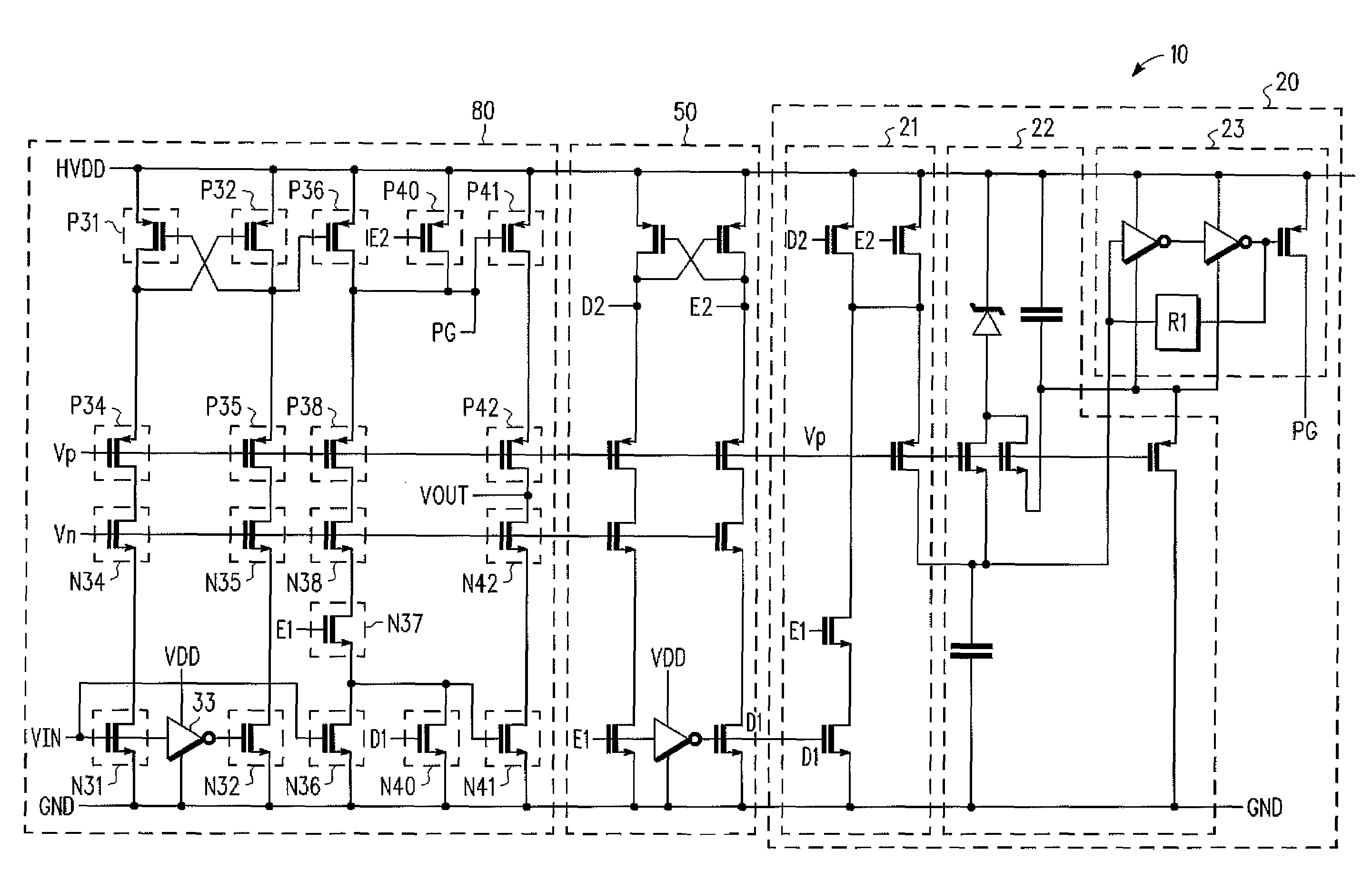
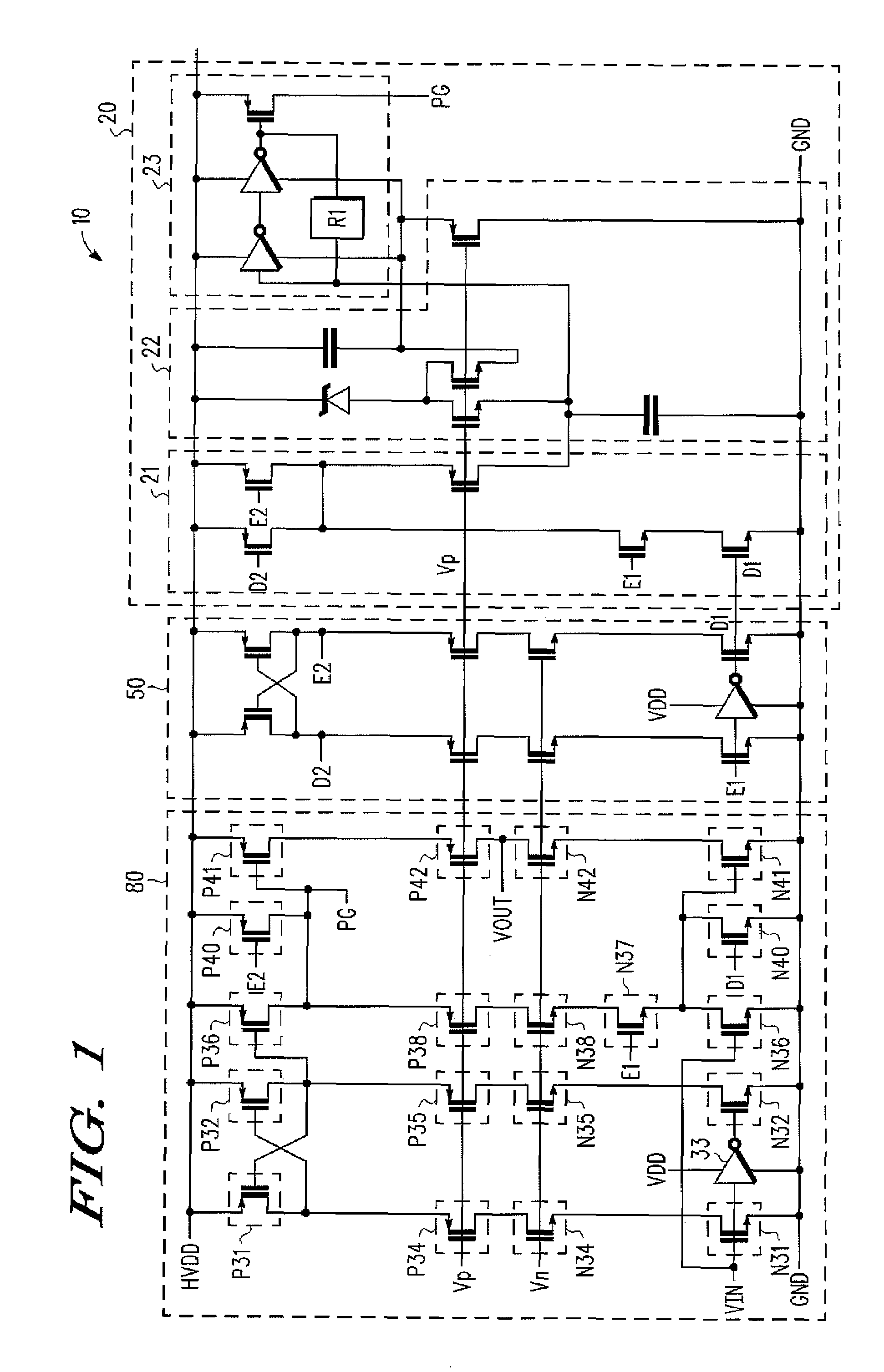
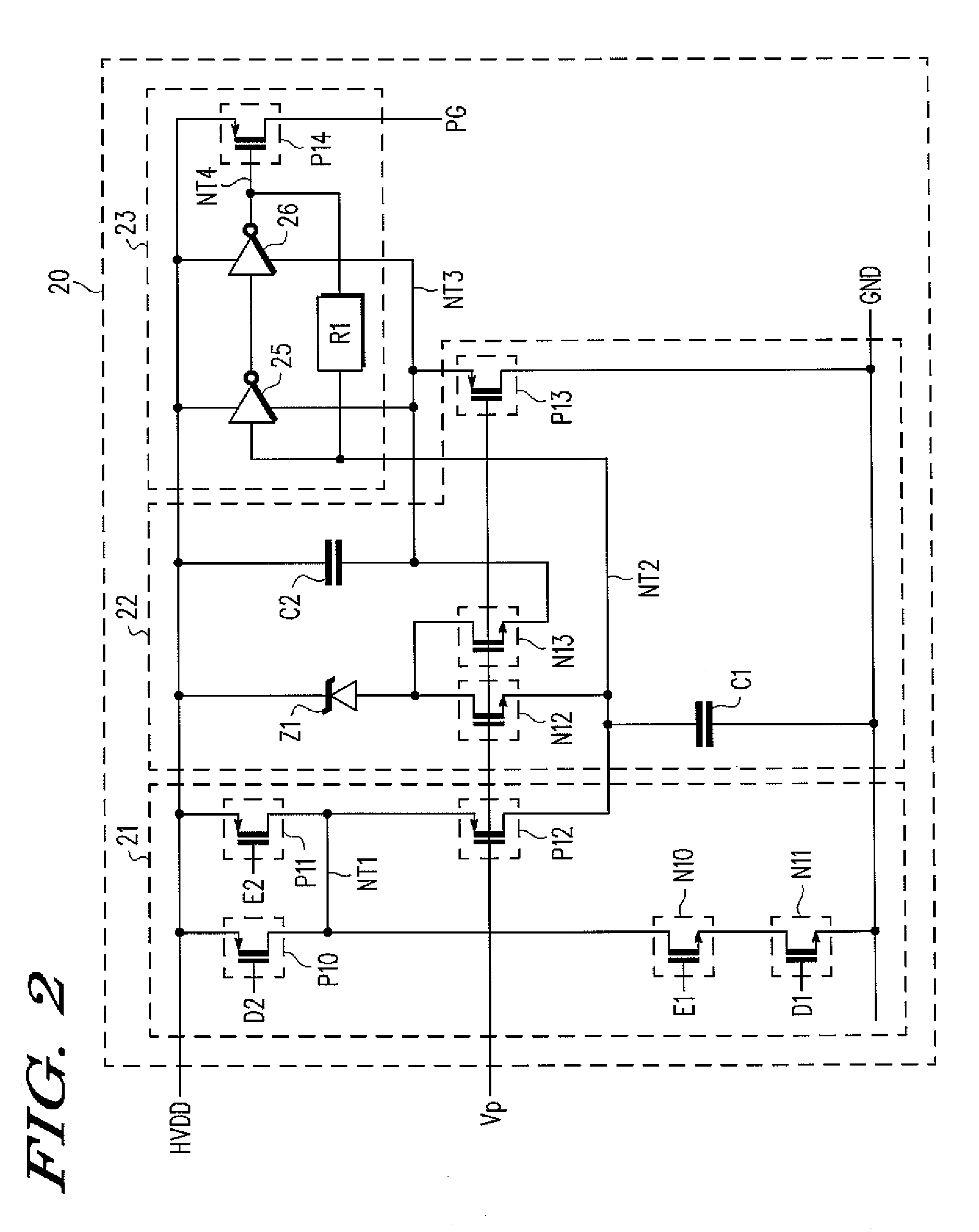
[0043]A level shifter circuit 10 according to a preferred embodiment of the present invention will now be described with reference to FIGS. 1 to 3. In the level shifter circuit 10 of the preferred embodiment, like or same reference numerals are given to those components that are the same as the corresponding components in the level shifter circuit 100 shown in FIG. 4. Such components will not be described in detail.

[0044]FIG. 1 shows the level shifter circuit 10 of the preferred embodiment. The level shifter circuit 10 is in a high impedance state when provided with an output enable signal E1 having a low level and outputs a low level or high level signal corresponding to the input signal when provided with an output enable signal E1 having a high level (so-called three states).

[0045]The level shifter circuit 10 uses ground voltage GND serving as a reference voltage, low potential power supply voltage VDD, and high potential power supply voltage HVDD. Specifically, in the preferred ...


PUM


Abstract

A level shifter circuit for ensuring a high impedance state even in a transitional period such as when activating an external power supply while reducing power consumption. A latch circuit is set to a low level by a set circuit when a high potential power supply voltage increases. When the high potential power supply voltage exceeds a threshold voltage, a p-channel MOS transistor of the latch circuit is activated and the high potential power supply voltage is applied to a first transistor via a connection node. When a high potential enable signal having normal high level signal voltage is provided to a second transistor, which is connected to the first transistor, the reset circuit provides the high level signal to the latch circuit and stops the voltage application to the first transistor via the connection node.

Description

BACKGROUND OF THE INVENTION[0001]The present invention relates to a level shifter circuit for converting a voltage of a high level input signal into a high voltage in accordance with the input signal and outputting the high voltage and for further outputting a high impedance state using an output enable signal.[0002]A level shifter circuit is known as a circuit for converting a low voltage signal to a high voltage signal. The level shifter circuit includes a circuit that performs a three-state output. The three states include low level output performed in accordance with the input level, high level output performed in accordance with the input level, and high impedance state output. The level shifter circuit for outputting three states includes a circuit that uses an output enable signal to determine whether to perform an output corresponding to the input level or a high impedance state output (refer to, for example, FIG. 1 of Japanese Laid-Open Patent Publication No. 2005-33530, an...

Claims


Application Information

Patent Timeline
Patent Type & Authority Patents(United States)
IPC IPC(8): H03K19/0175
CPCH03K19/018528
Inventor KIMURA, HIROYUKI
Owner NORTH STAR INNOVATIONS
Why Eureka
Try Eureka