Static random access memory (SRAM) with clamped source potential in standby mode

a random access memory and source potential technology, applied in static storage, information storage, digital storage, etc., can solve the problems of increased power consumption of sram and failure to screen

Inactive Publication Date: 2008-06-03
KK TOSHIBA
View PDF2 Cites 86 Cited by
  • Summary
  • Abstract
  • Description
  • Claims
  • Application Information

AI Technical Summary

Problems solved by technology

Along with a reduction in size and a reduction in voltage of LSIs, the SRAM is suffering an increase in power consumption by the leakage current in the standby mode.
Even if the external power supply is simply decreased, screening fails.

Method used


Image

  • Static random access memory (SRAM) with clamped source potential in standby mode
  • Static random access memory (SRAM) with clamped source potential in standby mode
  • Static random access memory (SRAM) with clamped source potential in standby mode

Examples


first embodiment

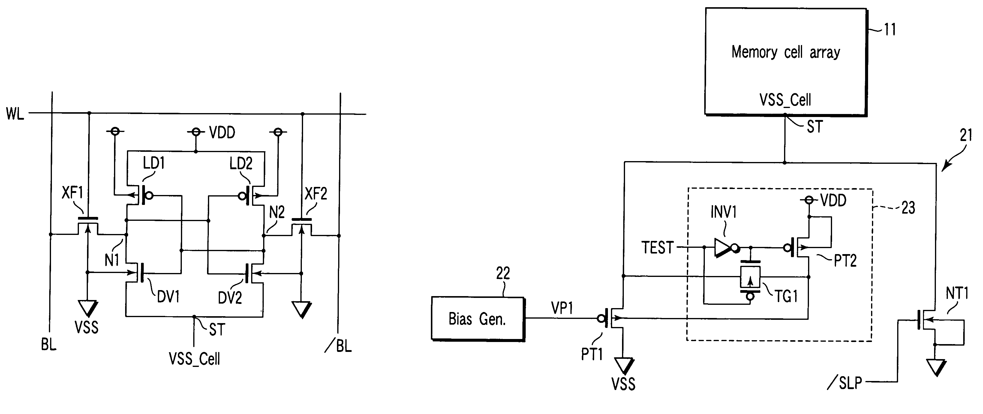
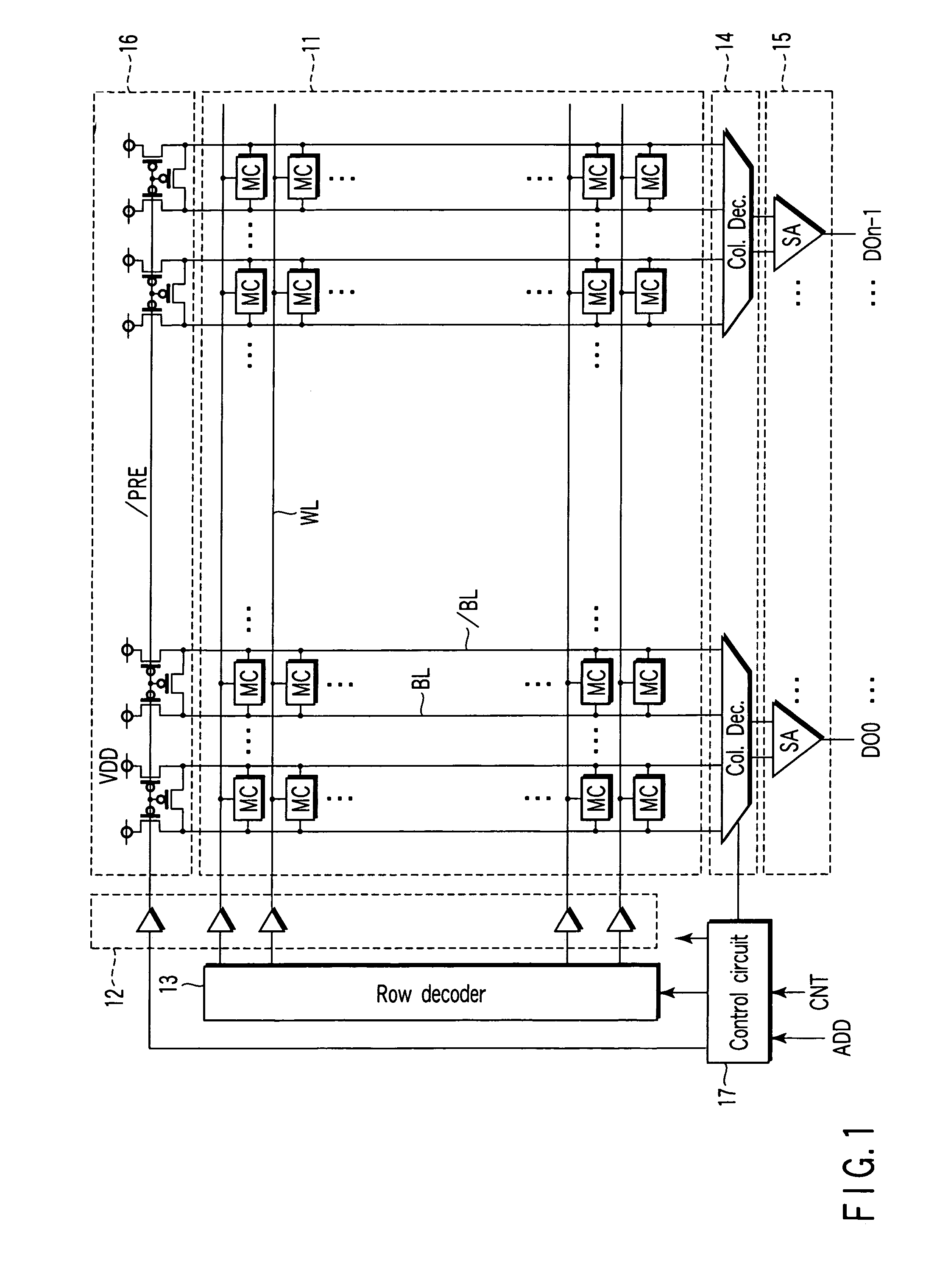
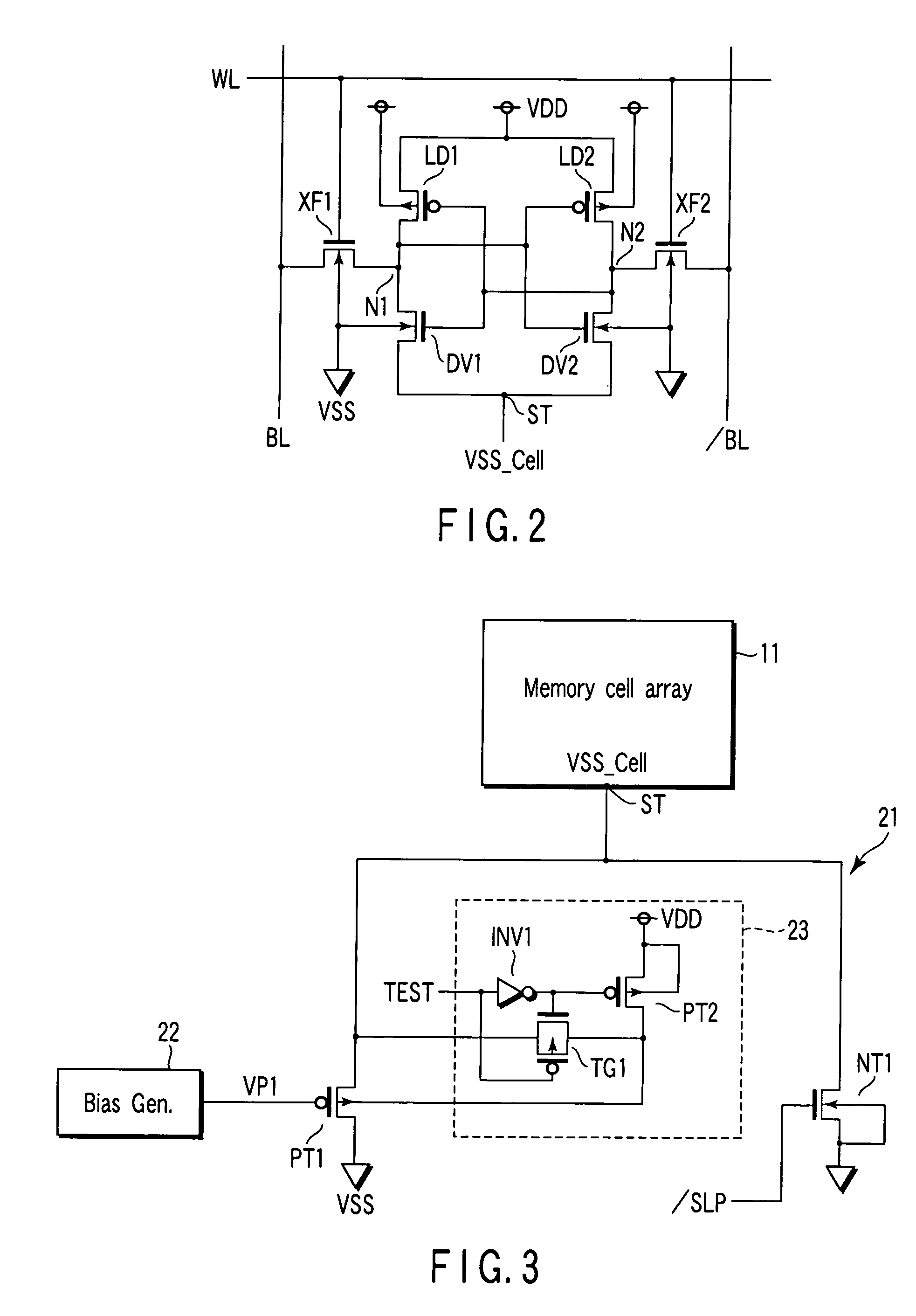
[0052]FIG. 1 is a block diagram illustrating an SRAM according to the first embodiment of the present invention. The SRAM comprises a memory cell array 11 which includes a plurality of static memory cells MC arranged in a matrix. In the memory cell array 11, a plurality of word lines WL are arranged. The word lines WL extend the row direction. Also in the memory cell array 11, a plurality of pairs of bit lines BL and / BL are arranged. The pairs of bit lines BL and / BL extend the column direction. A row of the memory cell array 11 is selected by the word line WL. A column of the memory cell array 11 is selected by a pair of bit lines BL and / BL.

[0053]The word lines WL are connected to a row decoder 13 via a word line driver circuit 12. The row decoder 13 selects a corresponding one of the word lines WL on the basis of a row address signal.

[0054]The pairs of bit lines BL and / BL are connected to a column decoder (Col. Dec.) 14. The column decoder 14 selects a corresponding pair from t...

second embodiment

[0100]In the first embodiment, a PMOS transistor is used as the clamp MOS transistor. However, an NMOS transistor can also be used.

[0101]FIG. 8 is a circuit diagram illustrating a cell bias control circuit 21 according to the second embodiment of the present invention. A source terminal ST is connected to a clamp NMOS transistor NT2. The gate and drain terminals of the NMOS transistor NT2 are connected (diode-connected). The drain terminal of the NMOS transistor NT2 is connected to the source terminal ST. The source terminal of the NMOS transistor NT2 is connected to the ground potential VSS.

[0102]The back gate terminal of the NMOS transistor NT2 is connected to a level switching circuit 23 for switching the potential level of the back gate terminal. The level switching circuit 23 comprises NMOS transistors NT3 and NT4 and an inverter circuit INV1.

[0103]The source and back gate terminals of the NMOS transistor NT3 are connected to the back gate terminal of the NMOS transistor NT2. T...

third embodiment

[0108]In the first embodiment, the back gate terminal of the clamp PMOS transistor PT1 is set to the power supply potential VDD in the screening test mode. A screening test using the back bias effect can also be performed as far as the back gate terminal of the clamp PMOS transistor PT1 is at a level higher than the source potential VSS_Cell. In the third embodiment, the back gate terminal of the clamp PMOS transistor PT1 is set to a potential other than the power supply potential VDD in the screening test mode.

[0109]FIG. 9 is a circuit diagram illustrating a cell bias control circuit 21 according to the third embodiment of the present invention. A bias generation circuit 22 generates bias potentials VP1 and VB1. The bias potential VB1 is set to a potential (in the third embodiment, for example, an intermediate potential between the power supply potential VDD and the ground potential VSS) lower than the power supply potential VDD.

[0110]The input terminal of a transfer gate TG2 recei...


PUM


Abstract

A semiconductor memory device includes a memory cell array including a plurality of memory cells, a source terminal which supplies a source potential to the memory cells, a first switching element which electrically connects the source terminal and a first power supply potential in an operation mode of the memory cells, and electrically disconnects the source terminal and the first power supply potential in a standby mode of the memory cells, a clamp MIS transistor which is series-connected between the source terminal and the first power supply potential, and clamps the source potential in the standby mode, a bias generation circuit which supplies a first bias potential to a gate terminal of the clamp MIS transistor, and a switching circuit which switches a potential of a back gate terminal of the clamp MIS transistor between a test mode and a non-test mode.

Description

CROSS-REFERENCE TO RELATED APPLICATIONS[0001]This application is based upon and claims the benefit of priority from prior Japanese Patent Application No. 2005-373516, filed Dec. 26, 2005, the entire contents of which are incorporated herein by reference.BACKGROUND OF THE INVENTION[0002]1. Field of the Invention[0003]The present invention relates to a semiconductor memory device and semiconductor integrated circuit and, more particularly, to an SRAM (Static Random Access Memory) including a static memory cell.[0004]2. Description of the Related Art[0005]SRAMs are widely used in general LSIs (Large-Scale Integrated circuits). Along with a reduction in size and a reduction in voltage of LSIs, the SRAM is suffering an increase in power consumption by the leakage current in the standby mode.[0006]More specifically, an SRAM cell has two load P-channel MOS (Metal Oxide Semiconductor) transistors and two driving N-channel MOS transistors. The SRAM cell stores data by turning on / off these MO...

Claims


Application Information

Patent Timeline
Patent Type & Authority Patents(United States)
IPC IPC(8): G11C5/14G11C11/413G11C29/00
CPCG11C7/1051G11C29/50G11C11/41G11C2207/108G11C2207/2227
Inventor HIRABAYASHI, OSAMU
Owner KK TOSHIBA
Why Eureka
Try Eureka