Optically oriented three-dimensional polymer microstructures

a three-dimensional polymer and microstructure technology, applied in the field of three-dimensional polymer microstructures, can solve the problems of limiting structure, preventing scalability, and advancing process still relies on a complicated and time-consuming layer-by-layer approach

Active Publication Date: 2008-06-03
HRL LAB
View PDF29 Cites 286 Cited by
  • Summary
  • Abstract
  • Description
  • Claims
  • Application Information

AI Technical Summary

Benefits of technology

[0008]An aspect of the present invention provides a method and system of fabricating polymer cellular (porous) materials with an ordered three-dimensional (3D) microstructure using a simple technique. These cellular materials are created from a pattern of self-propagating polymer waveguides, which are formed in an appropriate photopolymer. This method and system can create truly 3D microstructures without building the structures layer-by-layer as with stereolithography and other prototyping techniques.

Problems solved by technology

Techniques do exist to create polymer materials with ordered 3D microstructures, such as stereolithography techniques; however, these techniques rely on a bottom-up, layer-by-layer approach which prohibits scalability.
However, this advance process still relies on a complicated and time consuming layer-by-layer approach.
3D ordered polymer cellular structures have also been created using optical interference pattern techniques, also called holographic lithography; however, structures made using these techniques have an ordered structure at the nanometer scale and the structures are limited to the possible interference patterns, as described in Campbell et al., “Fabrication Of Photonic Crystals For The Visible Spectrum By Holographic Lithography,” NATURE, Vol. 404, Mar. 2, 2000, which is incorporated by reference herein in its entirety.
The existing techniques to create polymer optical waveguides have only allowed one or a few waveguides to be formed and these techniques have not been used to created a self-supporting three-dimensional structure by patterning polymer optical waveguides.

Method used


Image

  • Optically oriented three-dimensional polymer microstructures
  • Optically oriented three-dimensional polymer microstructures
  • Optically oriented three-dimensional polymer microstructures

Examples


example

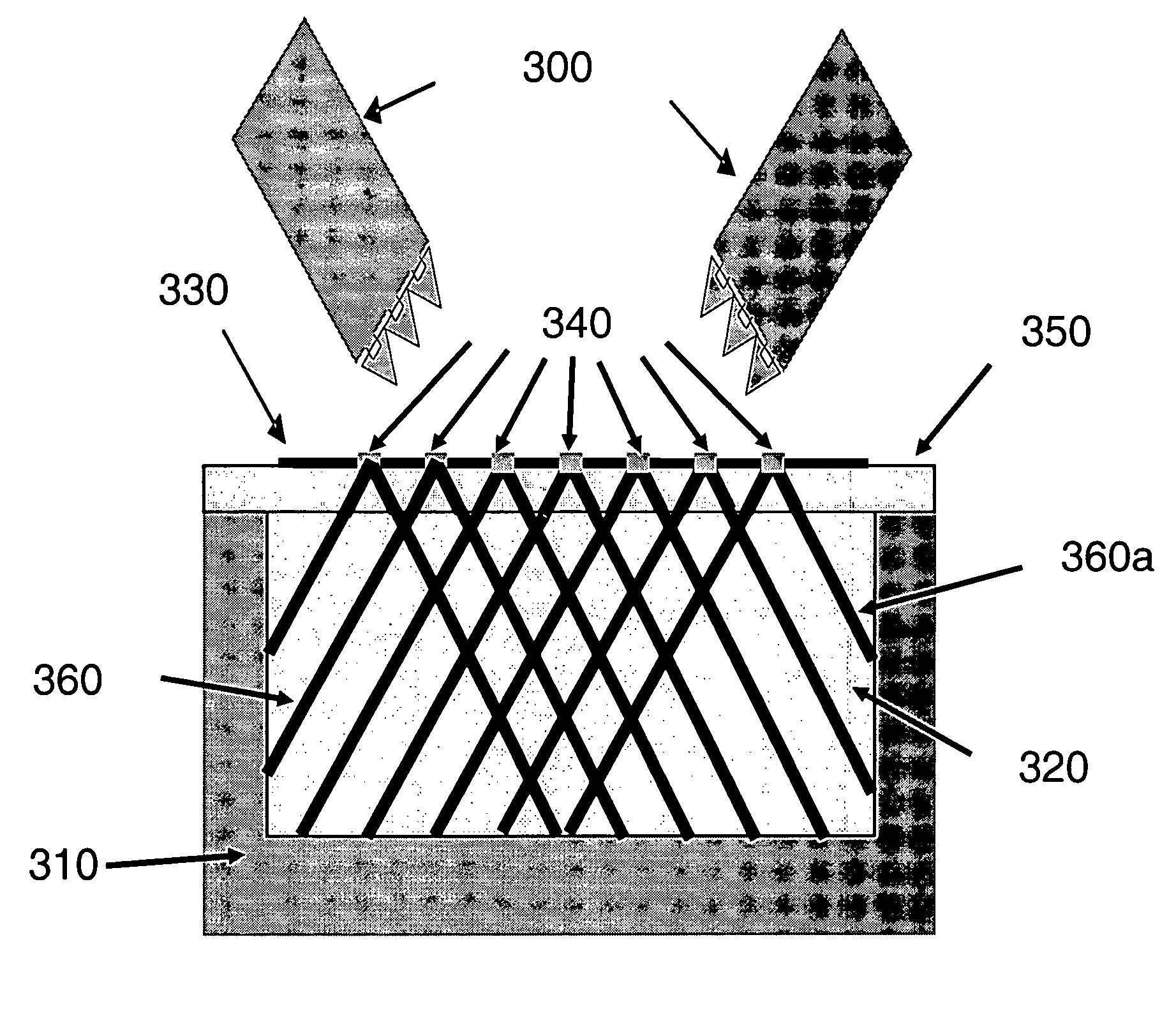
[0064]In forming a 3D polymer structure, a mold with an open top is filled with a monomer that will polymerize in the UV regime. The depth of this mold cavity is approximately 6 mm and was filled with a commercial photo-monomer. This commercial photo-monomer polymerizes via free-radical polymerization when exposed to UV light (wavelength between 250-400 nm), and is highly transmissive to light in this wavelength range—a property required for the formation of polymer waveguides. Non-limiting examples of the photo-monomer include any suitable free-radical photopolymer materials, such as urethanes (polyurethanes), acrylates, methacrylates, cationic polymers, such photo-cured epoxies, etc.

[0065]A glass substrate that is substantially transparent to UV light is placed on the top surface of the monomer and a Mylar mask is placed on top of the substrate (e.g., see FIG. 4). For this embodiment, the substrate is used to provide space between the mask and the monomer so the polymerized cellul...


PUM

PropertyMeasurementUnit
depthaaaaaaaaaa
wavelength rangeaaaaaaaaaa
diameteraaaaaaaaaa

Abstract

A method and system of creating one or more waveguides and / or patterning these waveguides to form a 3D microstructure that uses mask and collimated light. In one embodiment, the system includes at least one collimated light source selected to produce a collimated light beam; a reservoir having a photo-monomer adapted to polymerize by the collimated light beam; and a mask having at least one aperture and positioned between the at least one collimated light source and the reservoir. Here, the at least one aperture is adapted to guide a portion of the collimated light beam into the photo-monomer to form the at least one polymer waveguide through a portion of a volume of the photo-monomer.

Description

FIELD OF THE INVENTION[0001]The present invention relates to patterning one or more polymer waveguides to form an ordered three-dimensional (3D) microstructure and / or a system and method to fabricate the one or more polymer waveguides.BACKGROUND OF THE INVENTION[0002]An ordered three-dimensional (3D) microstructure is an ordered 3D structure at the micrometer scale. Currently, polymer cellular materials that are mass produced are created through various foaming processes, which all yield random (not ordered) 3D microstructures. Techniques do exist to create polymer materials with ordered 3D microstructures, such as stereolithography techniques; however, these techniques rely on a bottom-up, layer-by-layer approach which prohibits scalability.[0003]A stereolithography technique is a technique that builds a 3D structure in a layer-by-layer process. This process usually involves a platform (substrate) that is lowered into a photo-monomer (photopolymer) bath in discrete steps. At each s...

Claims


Application Information

Patent Timeline
Patent Type & Authority Patents(United States)
IPC IPC(8): G02B6/10G03C5/00G03C5/04
CPCB82Y20/00G02B1/005G02B6/1221G02B6/1225G02B6/138G03F7/0005G03F7/0037G03F7/201G03F7/2012G02B6/10
Inventor JACOBSEN, ALAN J.
Owner HRL LAB
Why Eureka
Try Eureka