Apparatus for inspecting wafer surface, method for inspecting wafer surface, apparatus for judging defective wafer, method for judging defective wafer, and apparatus for processing information on wafer surface

Inactive Publication Date: 2008-06-03
SUMCO TECHXIV
View PDF20 Cites 33 Cited by
  • Summary
  • Abstract
  • Description
  • Claims
  • Application Information

AI Technical Summary

Benefits of technology

[0011]In order to achieve the abovementioned first object, the wafer surface inspection device of the present invention is a device which detects aggregation of clustered fine point defects (LP

Problems solved by technology

The recognition of such LPD as linear scratches or staining from the two-dimensional state of aggregation of these LPD, and the performance of an inspection similar to an inspection performed by a human being in order to determine whether or not such scratches and staining are cause for a judgement of “defective”, have proved to be difficult.
Accordingly, it is necessary for a worker to examine this

Method used


Image

  • Apparatus for inspecting wafer surface, method for inspecting wafer surface, apparatus for judging defective wafer, method for judging defective wafer, and apparatus for processing information on wafer surface
  • Apparatus for inspecting wafer surface, method for inspecting wafer surface, apparatus for judging defective wafer, method for judging defective wafer, and apparatus for processing information on wafer surface
  • Apparatus for inspecting wafer surface, method for inspecting wafer surface, apparatus for judging defective wafer, method for judging defective wafer, and apparatus for processing information on wafer surface

Examples


Embodiment Construction

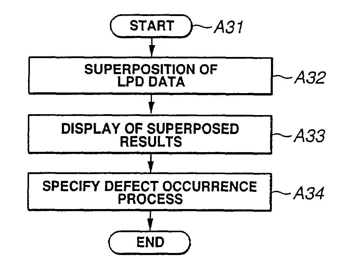
[0095]The wafer surface inspection device, wafer surface inspection method, defective wafer judgment device, defective wafer judgment method and wafer surface information processing device of the present invention will be described below with reference to the attached figures.

[0096]First, the wafer surface inspection device, wafer surface inspection method, defective wafer judgment device and defective wafer judgment method will be described.

Construction of the Apparatus

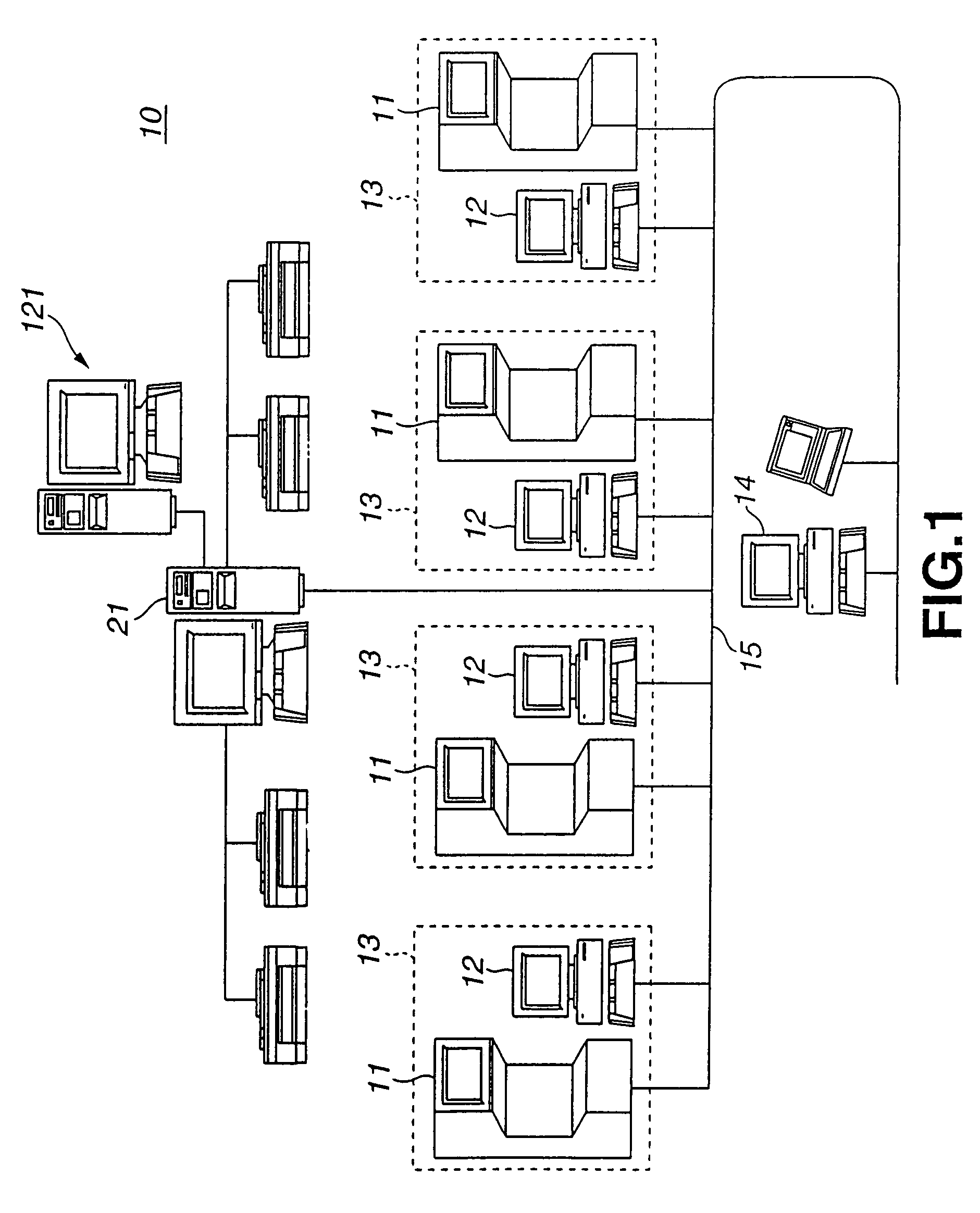
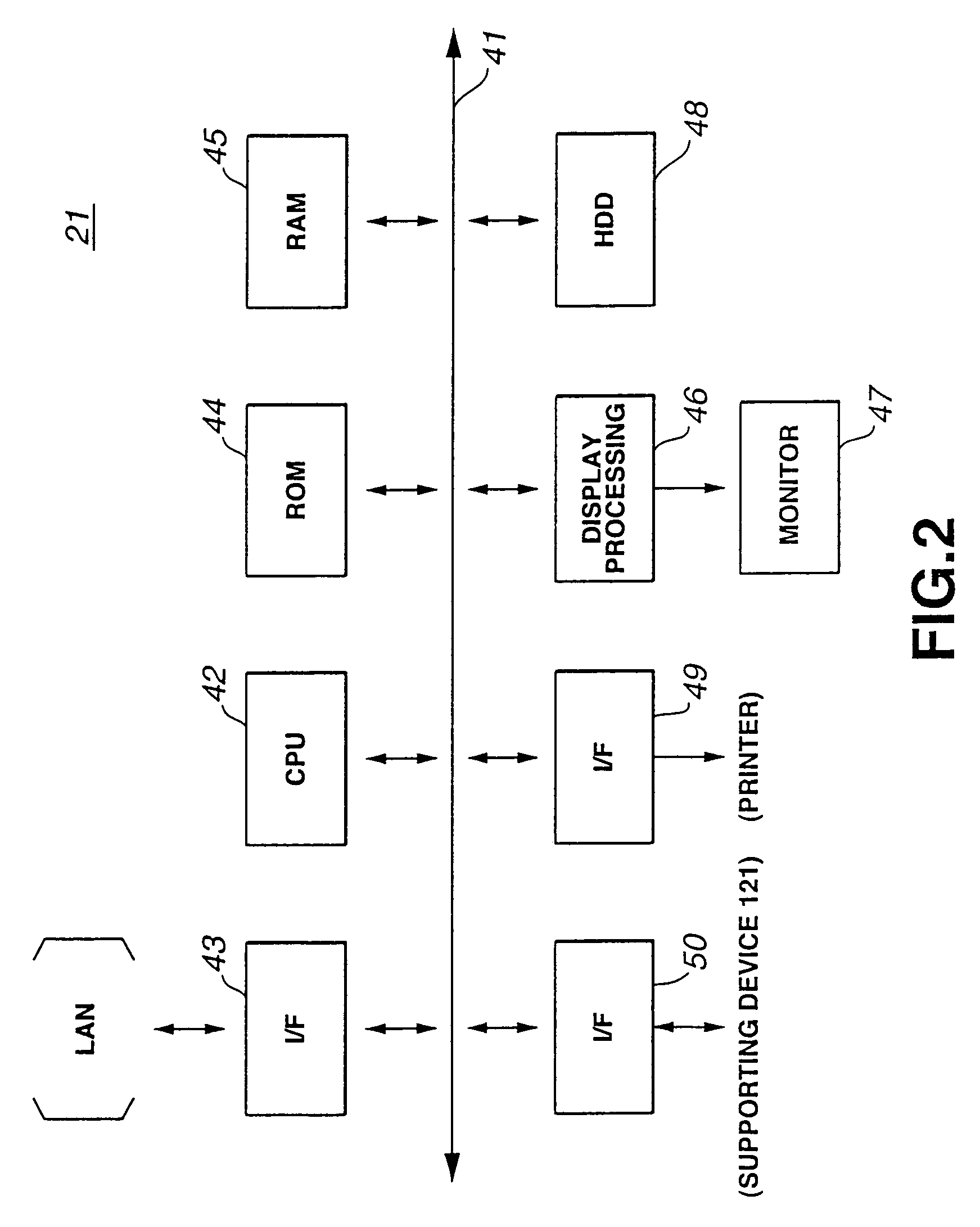
[0097]FIG. 1 is a schematic diagram which shows the overall construction of the wafer surface inspection system 10 of the present invention. As is shown in this FIG. 1, the wafer surface inspection system 10 has a plurality of extraction parts 13, each consisting of a laser scattering detector 11 that is used to extract fine defects from the surface of a silicon wafer, and a control computer 12 which is used to control this laser scattering detector 11; furthermore, the system has a judgement computer 21 which gather...


PUM


Abstract

It is possible to inspect scratches and staining on a wafer surface on the basis of an LPD map obtained from a particle counter 11, by providing a means 21 for detecting aggregation of clustered point defects (LPD) from two-dimensional distribution information 30 for such fine LPD on the surface of a silicon wafer, and an improvement in the inspection efficiency and the precision of judgements of “defective” status can be achieved. Furthermore, the system is devised so that the trend of generation of scratches and staining in a specified process can easily be detected by accumulating wafer surface information such as scratch information, staining information and the like for the wafer surface detected by a wafer surface inspection device 11 (especially as image information or numerical information), and superposing sets of information thus accumulated. Plans for improving processes can be made by both the wafer supplier and wafer consumer by sharing such information with both parties.

Description

TECHNICAL FIELD[0001]The present invention relates to a wafer surface inspection device and method which makes it possible to extract and classify defects such as scratches, staining and the like in a device that inspects the surfaces of silicon wafers for the presence or absence of scratches and staining. Furthermore, the present invention also relates to a judgement device and method which make it possible to perform judgements in accordance with the types of defects such as scratches, staining and the like in a device that judges defective wafers on the basis of scratches and staining on the surfaces of silicon wafers. Moreover, the present invention relates to a wafer surface information processing device which is used to accumulate wafer surface scratch information and staining information detected by the wafer surface inspection device, and to provide such information for use in wafer processing processes and other processes.BACKGROUND ART[0002]In silicon wafer manufacturing p...

Claims


Application Information

Patent Timeline
IPC IPC(8): G06F19/00G06F17/40G01N21/95G01N21/956H01L21/66
CPCG01N21/956H01L22/20G01N2021/8861
Inventor MATSUSITA, KOUZOUMATSUMURA, YUKINORITANUKI, TOMIKAZUTERADA, MITSUOHORI, KOTAROMIYAKAWA, KIYOHARUNISI, AKIRAMIWA, HIROBUMI
Owner SUMCO TECHXIV
Why Eureka
Try Eureka