

Semiconductor integrated circuit device
a technology of integrated circuits and semiconductors, applied in the direction of static storage, digital storage, instruments, etc., can solve the problems of many blocks unused by users, reduced storage capacity, and difficult to carry out programs
- Summary
- Abstract
- Description
- Claims
- Application Information
AI Technical Summary
Benefits of technology
Problems solved by technology
Method used
Image

Examples
first embodiment
[0075]First, one example of an internal system executing a boot sequence will be described.
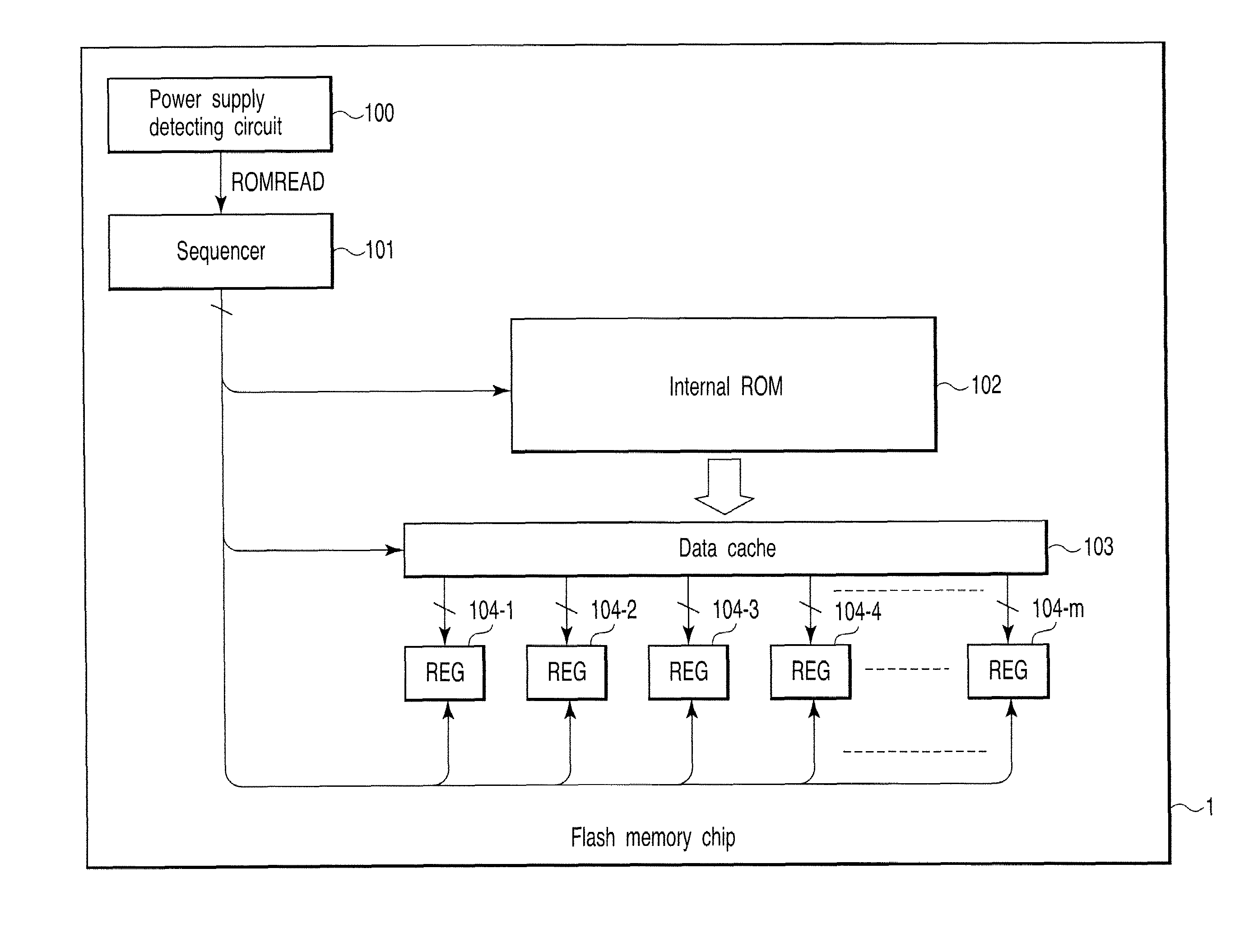
[0076]FIG. 3 is a block diagram showing one example of the internal system executing a boot sequence, which is provided in a semiconductor integrated circuit device according to the first embodiment of the present invention.
[0077]As shown in FIG. 3, the internal system executing a boot sequence is built into a nonvolatile semiconductor memory chip, for example, a flash memory chip 1. One example of a flash memory is a NAND type flash memory. The internal system includes a power supply detecting circuit 100, a sequencer 101, an internal ROM 102, a data cache 103, and a register groups 104-1 to 104-m.
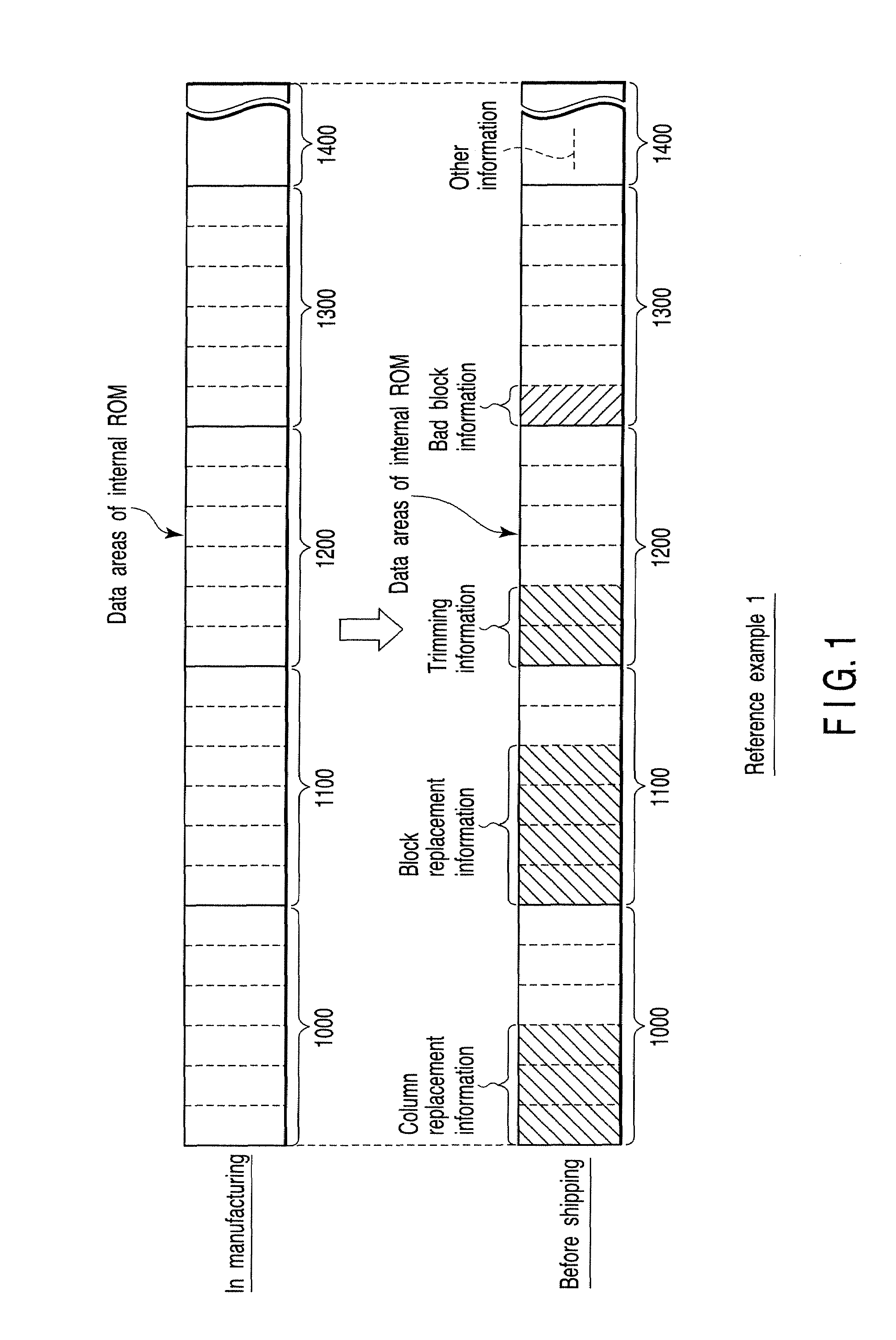
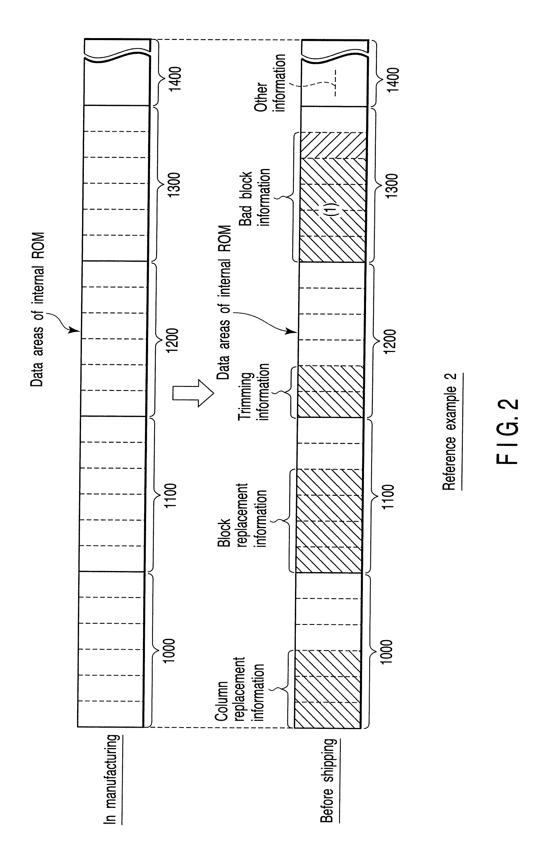
[0078]Information utilized for a boot sequence is registered with the internal ROM 102. The information utilized for a boot sequence includes column replacement information, block replacement information, trimming information, and bad block information in the present example. Other information may ...
second embodiment
[0098]Next, a concrete example of a semiconductor integrated circuit device in which it is possible to execute the example of the boot sequence described in the first embodiment will be described as a second embodiment.
[0099]FIG. 8 is a block diagram showing one example of the semiconductor integrated circuit device according to the second embodiment of the present invention. In the present example, a NAND type flash memory is shown as the semiconductor integrated circuit device.
[0100](Memory Cell Array: 201)
[0101]As shown in FIG. 8, the semiconductor integrated circuit device has a memory cell array 201. The memory cell array 201 is a portion of a main memory of a NAND type flash memory. In the memory cell array 201, nonvolatile semiconductor memory cells are disposed in a matrix form. One example of a nonvolatile semiconductor memory cell is a flash memory cell. A concrete example of the memory cell array 201 is shown in FIG. 9.
[0102]As shown in FIG. 9, the memory cell array 201 i...
third embodiment
[0177]FIG. 20 is a signal waveform diagram showing one example of signal waveforms when address information of the defective block is transferred to the block address register, in a semiconductor integrated circuit device according to a third embodiment of the present invention.
[0178]The third embodiment is different from the second embodiment in that the address information of the defective block is transferred in parallel to the BRD registers 401 and the block address register 405.
[0179]As shown in FIG. 20, in the present embodiment, during a sequence BRD_LOAD in which the address information of the defective block is transferred, a gate signal A permitting a data output to the internal bus 402 is activated, and a gate signal Bin permitting an input to the BRD registers 401, and a gate signal C permitting an input to the block address register 405 are activated. In accordance therewith, it is possible to transmit the same data simultaneously to both of the BRD registers 401 and th...
PUM
 Abstract
Description
Claims
Application Information