Integrated microfluidic array device

Active Publication Date: 2008-06-24
AGILENT TECH INC
View PDF22 Cites 99 Cited by
  • Summary
  • Abstract
  • Description
  • Claims
  • Application Information

AI Technical Summary

Benefits of technology

[0017]In one embodiment, the microfluidic component and the array component each have a substantially smooth interface surface, so that the interface surfaces may be joined to create a fluid-tight seal between the microfluidic component and the array component. In some embodiments a top layer disposed over the array component may be removed after the array is exposed to a sample containing target molecules, allowing access to the array for more effectively washing and/or interrogating the array without interference from the top layer. In an embodiment, the microfluidic component includes a microfluidic channel defined by a flexible, extendable sipper structure such as that described in the U.S. patent application Ser. No. 09/981,840 to Barth et al. (filed on Oct. 17, 2001), wherein the microfluidic channel is in fluid communication with an array surface of the array component.
[0018]The invention provides for integrated devices having a fluid containment structure such as a chamber, an array on a flexible substrate disposed within the chamber, and a microfluidic feature in fluid communication with the fluid containment structure. The fluid containment structure serves to retain a sample in contact with the array, e.g. during the hybridization reaction. The microfluidic feature may serve to, e.g. supply the sample to the fluid containment structure, and other microfluidic features may be present, providing further capabilities, such as sample preparation, purification, digestion, mixing, etc. During use, the sample may be removed from the fluid containment structure via one or more of the microfluidic feature(s), and wash fluids may be introduced to the fluid containment structure via one or more of the microfluidic fea

Problems solved by technology

Glass has the disadvantages of being rigid and brittle and difficult to attach to other materials.
In array fabrication, the quantities of biomolecules available are usually very small and expensive.
Furthermore, precisely cutting a substrate, such as glass, after the expensive arrays have been fabricated on the substrate leads to some loss due to breakage.
Such array substrates may have numerous surface modifications, increasing the overall cost of the array.
Although a single photod

Method used


Image

  • Integrated microfluidic array device
  • Integrated microfluidic array device
  • Integrated microfluidic array device

Examples


Example

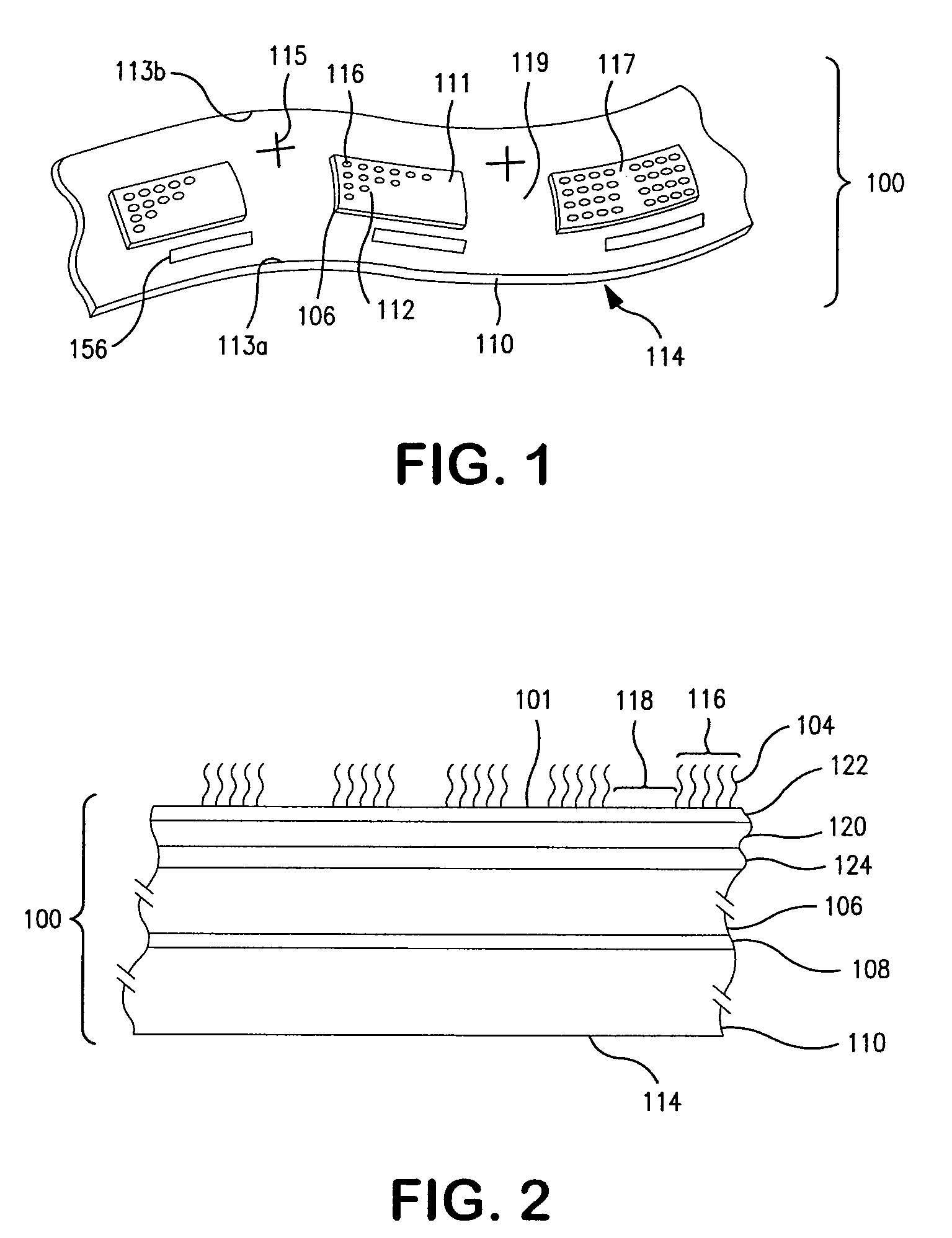
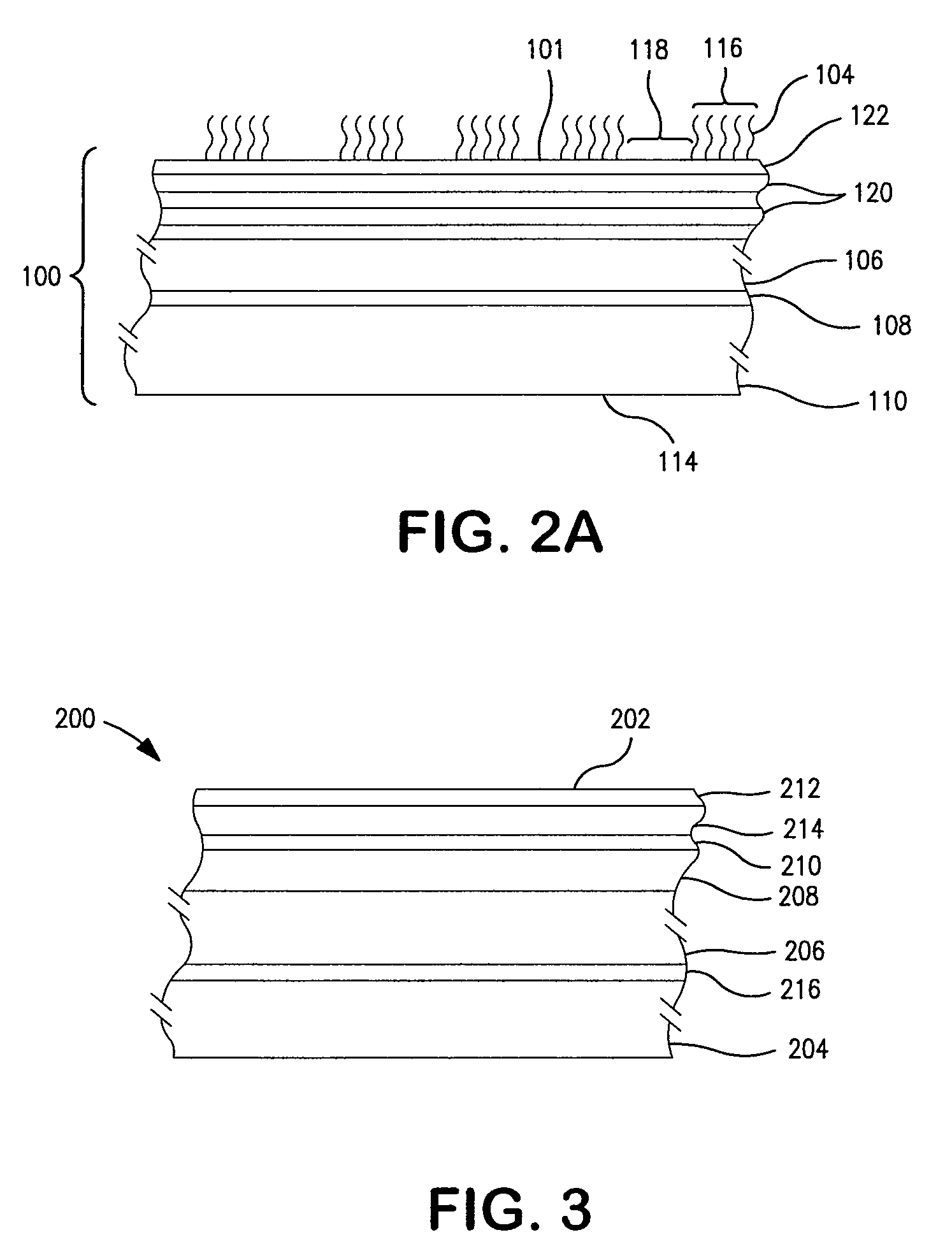
[0040]To facilitate understanding, identical reference numerals have been used, where practical, to designate corresponding elements that are common to the Figures. Figure components are not drawn to scale. To avoid cluttering the figures, certain features are illustrated numerous times to show representative presence of the feature, but not all instances of the features are explicitly illustrated. A particular example is the spots on an array. Also, certain illustrated features may be present at numerous places in a figure but only be labeled once or a few times by a reference numeral. Such unlabeled instances of features may be readily identified by referring to like features that are labeled in the figure. The figures may illustrate portions of larger compositions that comprise the features illustrated and are intended to be illustrative only.

DETAILED DESCRIPTION

[0041]Before the invention is described in detail, it is to be understood that unless otherwise indicated this inventio...


PUM

PropertyMeasurementUnit
Thicknessaaaaaaaaaa
Thicknessaaaaaaaaaa
Thicknessaaaaaaaaaa

Abstract

A microfluidic component having a microfluidic channel is joined to an array component having a flexible array substrate. In an embodiment, the array component includes a prefabricated flexible array that couples with the microfluidic component in modular fashion. The modular architecture provides for different combinations of microfluidic components and array components that can be used to create customized processing and analysis tools.

Description

RELATED APPLICATIONS[0001]This application is related to U.S. patent applications entitled “Device with Integrated Microfluidic and Electronic Components”, Ser. No. 10 / 286,319 “Composite Flexible Array Substrate Having Flexible Support”, Ser. No. 10 / 285,759; “Test Strips Including Flexible Array Substrates and Method of Hybridization” Ser. No. 10 / 286,117 “Device Having Multiple Molecular Arrays” Ser. No. 10 / 285,756 “Array Substrates Having Protective Layer” Ser. No. 10 / 286,090 all applications by Carol Schembri, all applications filed the same day as the instant application., all of which are incorporated herein by reference in their entireties.TECHNICAL FIELD[0002]The invention generally relates to microfabricated devices for chemical and biological analysis, and more particularly relates to integrated devices combining microfluidic features and arrays.BACKGROUND[0003]Arrays (such as DNA, RNA, or protein arrays) are known and are used, for example, as diagnostic or screening tools....

Claims


Application Information

Patent Timeline
IPC IPC(8): G01N21/00B01J19/00B01L3/00B29C65/00C40B60/14C40B70/00
CPCB01J19/0046B01L3/5027B01L3/505B29C65/00Y10T436/2575B01J2219/00518B01J2219/00529B01J2219/00547B01J2219/00596B01J2219/00608B01J2219/0061B01J2219/00612B01J2219/00621B01J2219/00626B01J2219/00637B01J2219/00662B01J2219/0072B01L3/502707B01L3/5085B01L2200/025B01L2200/10B01L2200/12B01L2200/143B01L2300/021B01L2300/0636B01L2300/0819B01L2300/0825B01L2300/0829B01L2300/0861B01L2300/0887B01L2300/123B01L2300/168C40B60/14C40B70/00B01J2219/00351B29C66/71B29K2077/00B29K2071/00B29K2067/003B29K2067/00B29K2033/12B29K2033/08B29K2027/18B29K2027/06B29K2025/06B29K2023/18B29K2023/12B29K2023/06B29K2023/00B29K2001/12
Inventor SCHEMBRI, CAROL T
Owner AGILENT TECH INC
Why Eureka
Try Eureka