

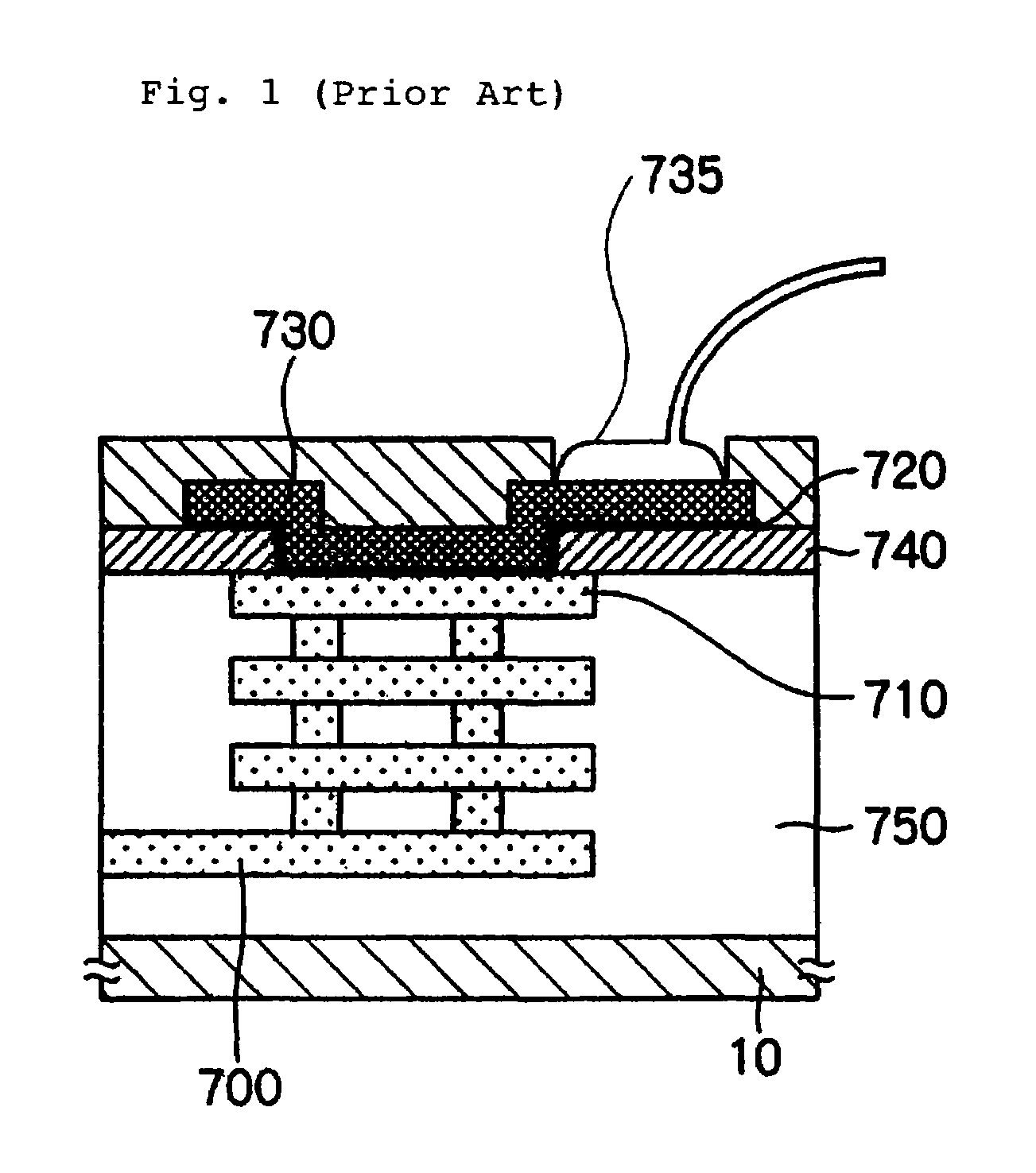
Semiconductor device with bonding pad support structure
a technology of support structure and semiconductor, which is applied in the direction of semiconductor devices, semiconductor/solid-state device details, electrical equipment, etc., can solve the problems of film peeling in the bonding pad, construction therefore tends to increase the chip size, etc., and achieve the effect of reducing the capacitance between copper layer patterns
- Summary
- Abstract
- Description
- Claims
- Application Information
AI Technical Summary
Benefits of technology
Problems solved by technology
Method used
Image

Examples
first working example
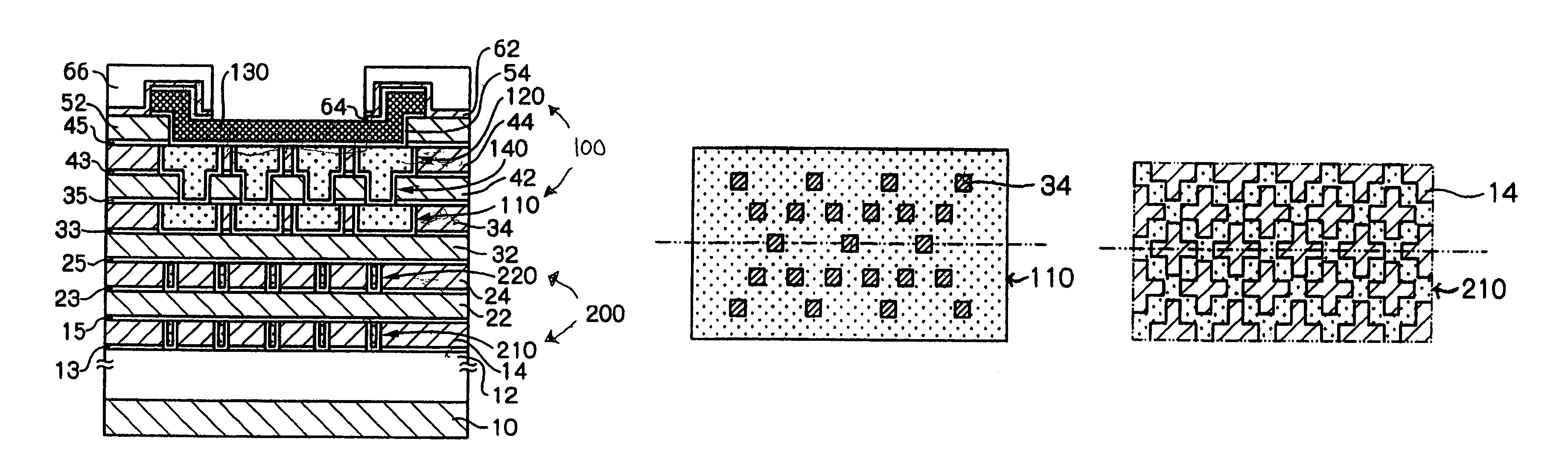
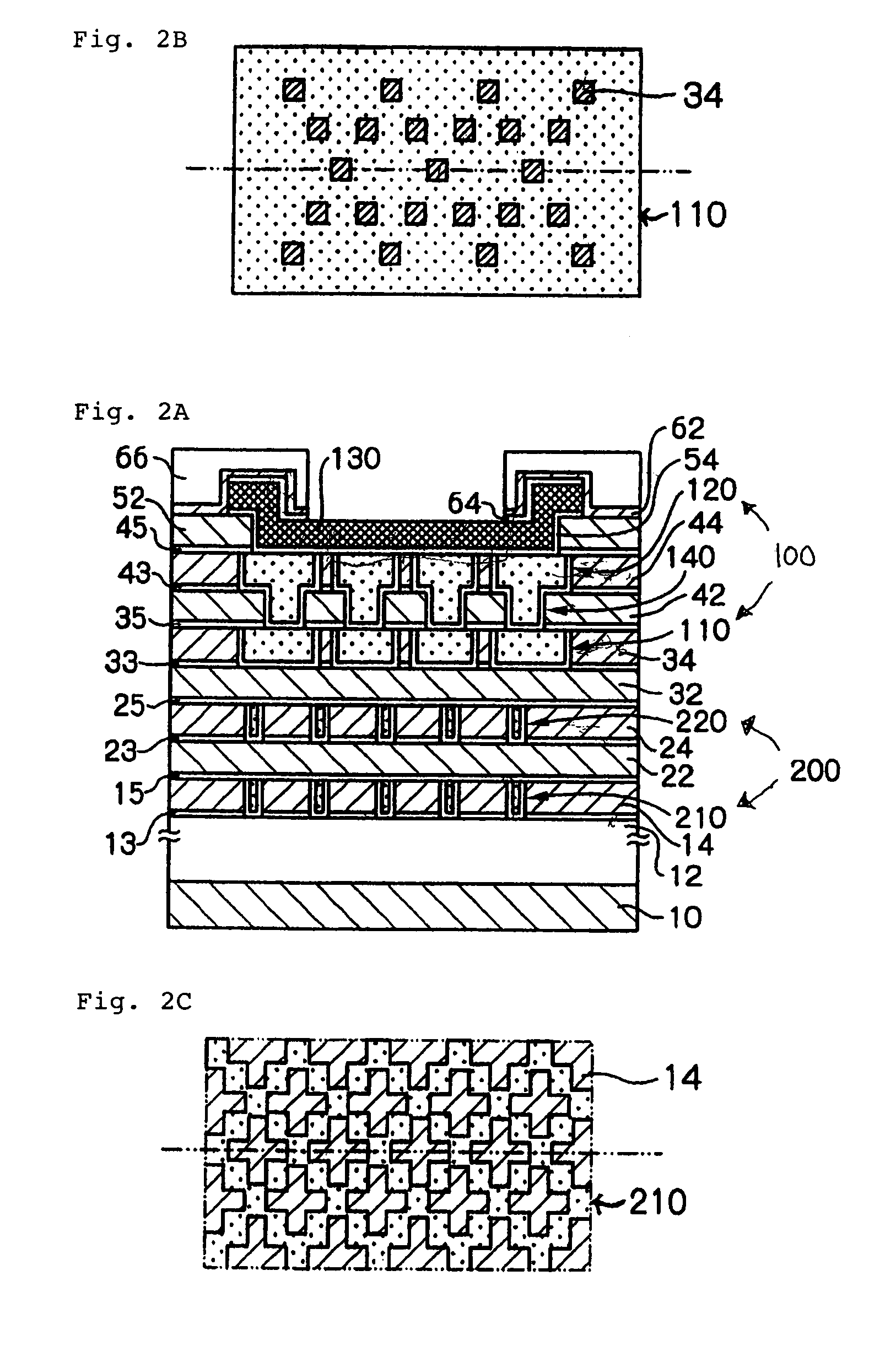
[0046]FIG. 2A is a sectional structural view showing the configuration of an area that includes a bonding pad of the semiconductor device that is the first working example of the present invention.
[0047]Referring now to FIG. 2A, the semiconductor device of the present working example includes upper copper layer 100 for improving shock resistance, this upper copper layer 100 being formed below bonding pad 130 that includes a metal film having aluminum (Al) as its chief component, a barrier metal being interposed between upper copper layer 100 and bonding pad 130. The barrier metal is provided for preventing the aluminum that is contained in bonding pad 130 from reacting with elements that are contained in the upper layer. Upper copper layer 100 and bonding pad 130 have substantially identical planar dimensions (meaning that the planar dimensions are identical within the range of fabrication error), and upper copper layer 100 uniformly supports bonding pad 130 from below.
[0048]To prov...
second working example
[0076]In the construction of the above-described first working example, the connection of the bonding pads and internal circuits is realized by way of the upper copper layer, but a construction is also possible in which the bonding pads are connected to auxiliary copper interconnects that are connected to the internal circuits. Explanation next regards a semiconductor device in which this type of connection structure is applied.
[0077]FIG. 3 is a sectional structural view of the semiconductor device that is the second working example of the present invention. As shown in FIG. 3, in the semiconductor device of this working example, auxiliary copper interconnect 125 that is connected to internal circuits is formed on the same level as second upper copper layer 120. Auxiliary copper interconnect 125 and bonding pad 130 are electrically connected by way of via-hole 150. The construction is otherwise basically the same as the construction of the above-described first working example.
[0078...
third working example
[0083]A plurality of bonding pads can be arranged in the construction of the above-described second working example. Explanation here regards a semiconductor device in which this type of construction is applied.
[0084]FIG. 4A is a plan view of the semiconductor device that is the third working example of the present invention, and FIG. 4B is a sectional view of the structure in along the double-dot-single-dash line A-A′ in FIG. 4A. In these figures, FIG. 4A and FIG. 4B, titanium nitride (TiN) film 64, silicon dioxide (SiO2) film 62, and polyimide film 66 that were shown in FIG. 2A are formed on bonding pads 130, but this construction is here omitted for the sake of expediency.
[0085]As shown in FIG. 4A, the semiconductor device of the present working example is a construction in which outer pads 132, which are bonding pads that are close to scribe line 600, and inner pads 134, which are bonding pads that are closer to the center of the chip than outer pads 132, are aligned along diffe...
PUM
| Property | Measurement | Unit |
|---|---|---|
| thickness | aaaaa | aaaaa |
| thickness | aaaaa | aaaaa |
| thickness | aaaaa | aaaaa |
Abstract
Description
Claims
Application Information