Slot antenna

a slot antenna and antenna technology, applied in the field of slot antennas, can solve the problems of difficulty in covering the entire aforementioned wide frequency band, difficulty in realizing an antenna which covers, and the problem of conventional slot antennas in terms of wideband-ness

Inactive Publication Date: 2008-07-08
PANASONIC CORP
View PDF10 Cites 15 Cited by
  • Summary
  • Abstract
  • Description
  • Claims
  • Application Information

AI Technical Summary

Benefits of technology

[0112]In Examples 1c and 1d, the center of gravity of the isosceles triangle was set at a point opposing the edge 237 or 239 of the ground conductor 12, respectively. Example 1c exhibited an operating band from 4.72 GHz to 7.05 GHz, and a bandwidth ratio of 39.6%. Example 1d exhibited an operating band from 4.04 GHz to 6.28 GHz, and a bandwidth ratio of 43.4%. From the characteristics of Examples 1c and 1d, it was found that introducing a loop line at the input terminal side of the feed line contributes to wideband operation on the high-frequency side of the band, and introducing a loop line at the leading open point side of the feed line contributes to wideband operation on the low-frequency side of the band. Each of Examples 1a, 1b, 1c, and 1d realizes a low-return operation with a bandwidth ratio which is wider than that of Comparative Example 1, thus proving the advantageous effects of the present invention. Table 2 shows a comparison between the characteristics of Examples 1a to 1d and the characteristics of Comparative Example 1.
of the present invention. Table 2 shows a comparison between the characteristics of Examples 1a to 1d and the characteristics of Comparative

Problems solved by technology

With such antennas, it is very difficult cover the entirety of the aforementioned wide frequency band.
One reason thereof is the difficulty to realize an antenna which covers the entirety of an ultrawideband (UWB) with the currently-available technology.
The aforementioned conventional slot antenna has a problem in terms of wideband-ness.
Firstly, the operating band of a usual slot antenna, which only has a single resonator structure within its structure, is restricted by the band of its resonance phenomenon.
Although the antenna of Japanese Laid-Open Patent Publication No. 2004-336328 realizes a wideband operation because of a capacitive reactance element being introduced in the slot, there is a problem in that an additional part such as a chip capacitor is required as the actual capacitive reactance element.
There is also a problem in that variations in the characteristics of the newly-introduced additional part may cause the antenna characteristics to vary.
Furthermore, according to the example disclosed in Japanese Laid-Open Patent Publication No. 2004-336328, there is also a problem associated with the band characteristics.
However, such a band is still insufficient, and a VSWR of about three cannot be considered as representing good return intensity characteristics.
Thus, according to the disclosure of Japanese Laid-Open Patent Publication No. 2004-336328, it is difficult to provide an antenna which attains low-return input matching characteristics in a ultrawide frequency band that is currently desired.
The method of Japanese Laid-Open Patent Publication No. 2004-23507 will prove extremely difficult in practice.
Specifically, since the feed line 261 intersects a number of slots between the input terminal and the leading open-end point, a considerable impedance mismatch is predicted.
In either case, it will be difficult for this structure to achieve a bandwidth ratio of several tens of % or more.
Thus, a structure which requires a large Ws value in order to obtain wideband characteristics will be difficult to be downsized by nature.

Method used


Image

  • Slot antenna
  • Slot antenna
  • Slot antenna

Examples


embodiments

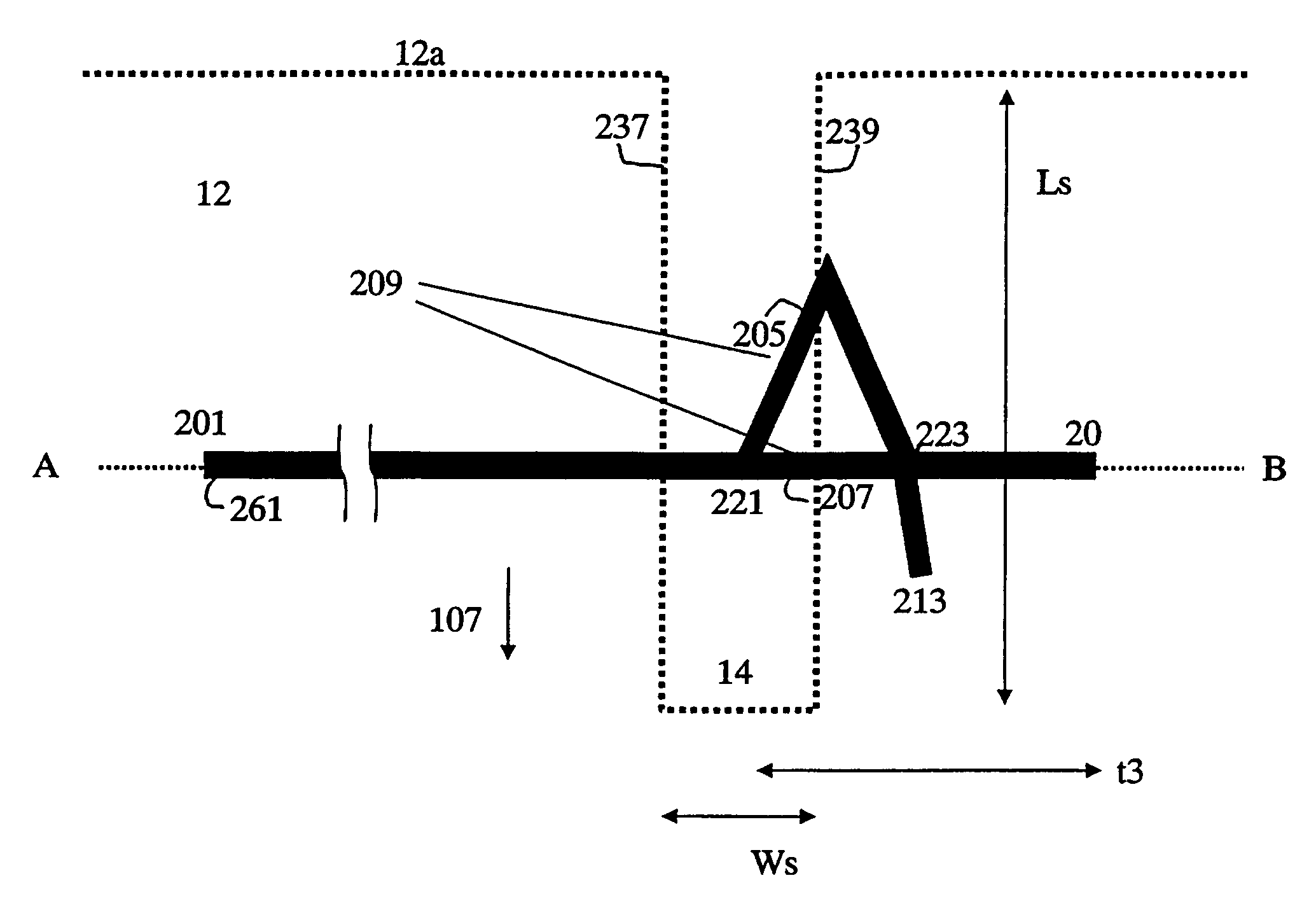
[0061]First, FIG. 1 is referred to. FIG. 1 is an upper schematic see-through view showing the structure of a slot antenna according to the present embodiment.

[0062]The slot antenna of the present embodiment includes a dielectric substrate 101 (FIG. 2), and a ground conductor 12 provided on the rear face of the dielectric substrate 101, the ground conductor 12 having a finite area. The ground conductor 12 has a slot 14, which is formed by recessing a side edge 12a of the ground conductor 12 in an inward direction 107. One end of the slot 14 is opened at the side edge 12a of the ground conductor 12, this end functioning as an “open-end point”. Assuming that the slot 14 has a slot width Ws which is negligible relative to the slot length Ls, the slot length Ls is prescribed equal to a ¼ effective wavelength near the center frequency f0 of the operating band. When this assumption is not true, a slot length which takes the slot width into consideration (Ls×2+Ws) may be prescribed equal to...

example

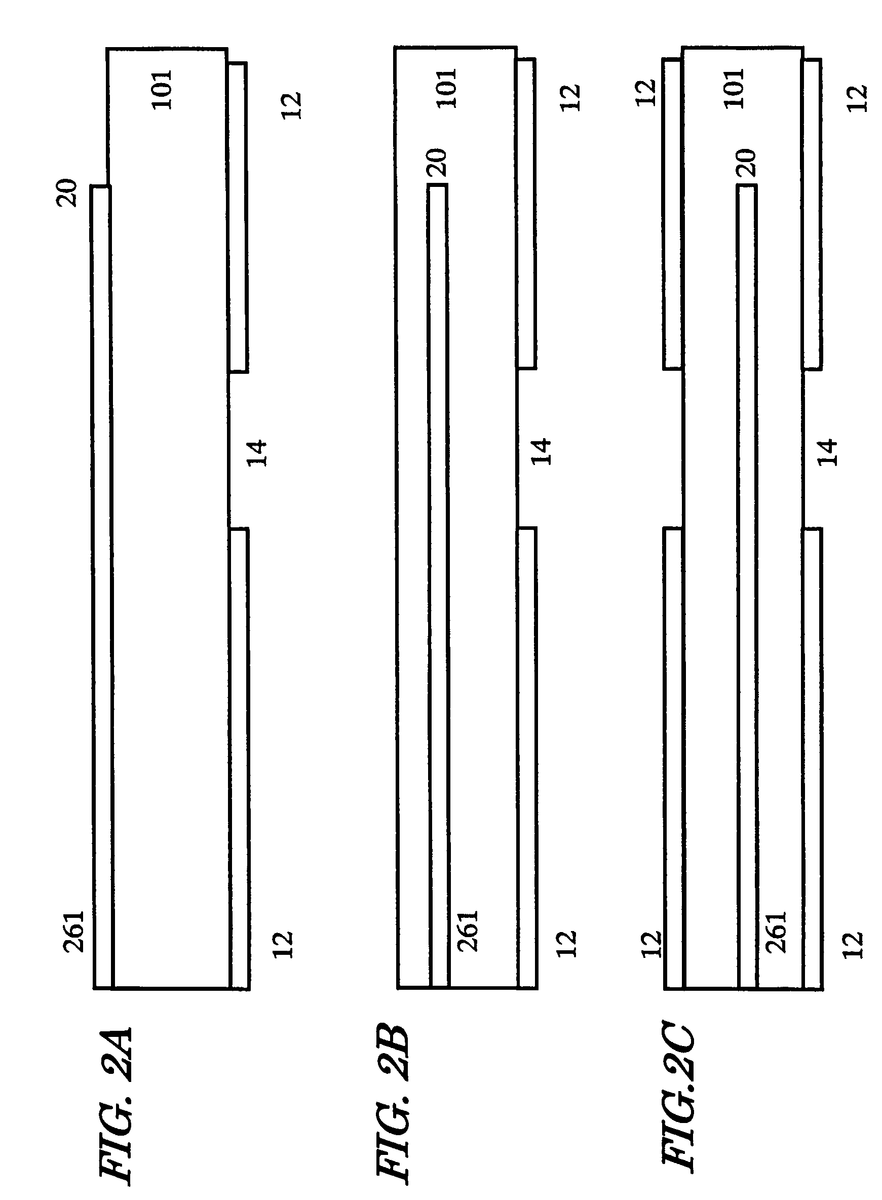
[0105]A slot antenna (Comparative Example 1) as shown in an upper schematic see-through view of FIG. 13 and a slot antenna (Example 1a) as shown in an upper schematic see-through view of FIG. 14 were produced. As a dielectric substrate 101, an FR4 substrate whose overall width was 500 microns and each of whose sides measured 60 mm (a=b=60 mm) was used. On the front face and the rear face of the substrate, a signal conductor pattern and a ground conductor pattern each having a thickness 20 microns were formed, respectively, by using a copper line. Each wiring pattern was formed by removing some regions of the metal layer through wet etching, and gold plating was provided on the surface to a thickness of 5 microns. An outer edge 12a of the ground conductor 12 remained inside the dielectric substrate 101, by no less than 100 microns, even at the closest points to the end faces of the dielectric substrate 101. In the figure, the ground conductor pattern is shown by a dotted line.

[0106]A...


PUM


Abstract

A slot antenna according to the present invention includes: a ground conductor 12 provided on a rear face side of a dielectric substrate 101, the ground conductor having a finite area; a slot 14 which recesses into the ground conductor 12, beginning from an open-end point on a side edge of the ground conductor 12; and a feed line 261 for supplying a high-frequency signal to the slot 14, the feed line 261 intersecting the slot 14. At a first point near the slot, the feed line 261 branches into a group of branch lines including at least two branch lines, such that at least two branch lines in the group of branch lines are connected to each other at a second point near the slot to form at least one loop line 209. A maximum value of a loop length of each loop line 209 is prescribed to be less than 1× effective wavelength at an upper limit frequency of an operating band of the slot antenna. In the group of branch lines, any branch line that does not constitute a part of the loop line 209 but terminates with a leading open-end point has a branch length which is less than a ¼ effective wavelength at the upper limit frequency of the operating band.

Description

[0001]This is a continuation of International Application No. PCT / JP2006 / 321541, with an international filing date of Oct. 27, 2006, which claims priority of Japanese Patent Application No. 2005-325674, filed on Nov. 10, 2005, the contents of which are hereby incorporated by reference.BACKGROUND OF THE INVENTION[0002]1. Field of the Invention[0003]The present invention relates to an antenna with which a digital signal or an analog high-frequency signal, e.g., that of a microwave range or an extremely high frequency range, is transmitted or received.[0004]2. Description of the Related Art[0005]For two reasons, wireless devices are desired which are capable of operating in a much wider band than conventionally. A first reason is the need for supporting short-range wireless communication systems, for which the authorities have given permission to use a wide frequency band. A second reason is the need for a single terminal device that is capable of supporting a plurality of communicatio...

Claims


Application Information

Patent Timeline
Patent Type & Authority Patents(United States)
IPC IPC(8): H01Q13/10H01Q5/10
CPCH01Q1/24H01Q1/38H01Q5/50H01Q5/25H01Q13/106
Inventor KANNO, HIROSHISAKIYAMA, KAZUYUKISANGAWA, USHIO
Owner PANASONIC CORP
Why Eureka
Try Eureka