
Oscillator

a technology of oscillator and oscillator body, which is applied in the direction of generating/distributing signals, pulse techniques, instruments, etc., can solve the problems of large circuit size, low precision, and inability to symmetrically configure the circuit configuration of the oscillator, and achieve the effect of simple configuration and high precision

Inactive Publication Date: 2008-07-22
SONY CORP
View PDF12 Cites 2 Cited by
  • Summary
  • Abstract
  • Description
  • Claims
  • Application Information

AI Technical Summary

Benefits of technology

This configuration enables the generation of even-numbered phases of clock signals with high precision, reducing circuit size and power consumption while minimizing jitter in the output clock signal.

Problems solved by technology

Further, processing for the selection is realized by a digital circuit, but when the number of phases of the multi-phase clock signals is an odd number, the arithmetic operations to be executed in the digital circuit become complex, so a processing circuit having a large circuit size is considered needed.
However, these oscillators do not have symmetry in circuit configuration.
From this, there is the problem that power supply noise is generated by fluctuation of the consumed current for every period in the oscillator, so a difference occurs in the phase difference between clock signals forming the multiple phases of clock signals.
However, a ring oscillator using inverters as components is large in circuit size.

Method used


Image

  • Oscillator
  • Oscillator
  • Oscillator

Examples


first embodiment

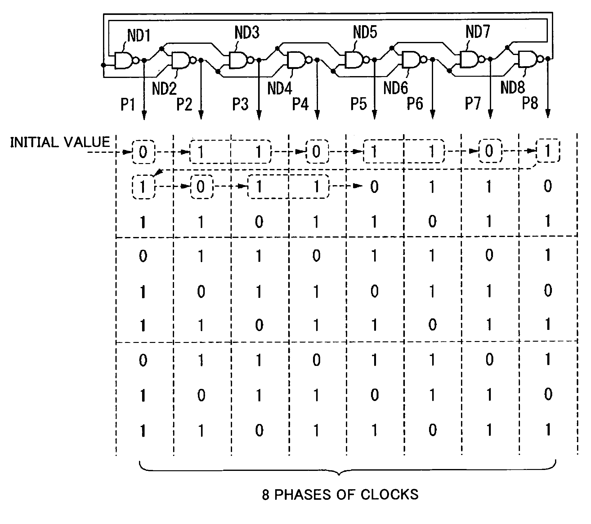
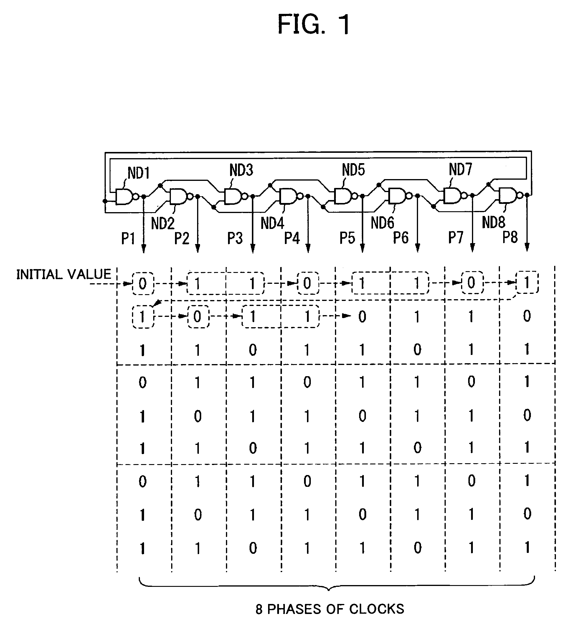
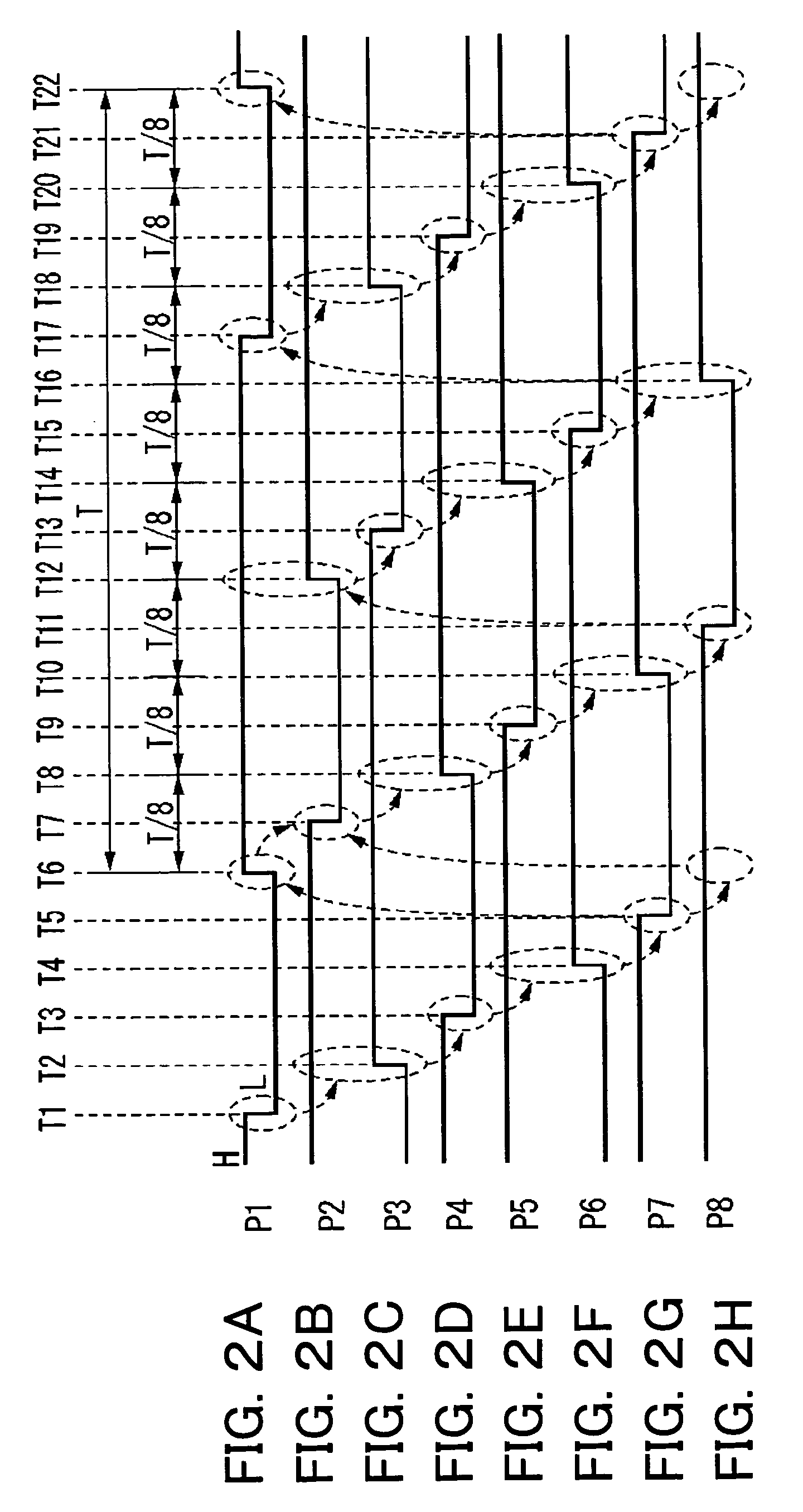
[0036]FIG. 1 is a view for explaining the configuration of an oscillator according to a first embodiment of the present invention and the operation thereof. As shown in FIG. 1, the oscillator according to the first embodiment is formed by eight NAND circuits ND1 to ND8 sequentially connected in a ring. Clock signals P1 to P8 are output from the output nodes of the NAND circuits ND1 to ND8.

[0037]Here, in the oscillator shown in FIG. 1, eight NAND circuits each having two input terminals are connected in a ring. The output node of each of the NAND circuits ND1 to ND8 is connected to one input node of each of the NAND circuits up to the NAND circuit exactly the number of input terminals' worth of places, that is, two places, ahead.

[0038]Namely, for example, the output node of the NAND circuit ND1 is connected to one input node of the NAND circuit ND2 connected one place ahead and one input node of the NAND circuit ND3 connected two places ahead. In the same way, the output node of the ...

second embodiment

[0061]FIG. 4 is a view for explaining the configuration of an oscillator according to a second embodiment of the present invention and the operation thereof. As shown in FIG. 4, the oscillator according to the second embodiment is formed by six NAND circuits ND11 to ND16 sequentially connected in a ring. Clock signals P1 to P6 are output from the output nodes of the NAND circuits ND11 to ND16.

[0062]Here, in the oscillator shown in FIG. 4, six NAND circuits each having three input terminals are connected in a ring. The output node of each of the NAND circuits ND11 to ND16 is connected to the input node of each of the NAND circuits up to the NAND circuit exactly the number of input terminals' worth of places, that is, three places, ahead.

[0063]Namely, for example, the output node of the NAND circuit ND11 is connected to one input node of the NAND circuit ND12 connected one place ahead, one input node of the NAND circuit ND13 connected two places ahead, and one NAND circuit ND14 connec...

third embodiment

[0080]FIG. 6 is a view for explaining the configuration of an oscillator according to a third embodiment of the present invention and the operation thereof. As shown in FIG. 6, the oscillator according to the third embodiment is formed by six NAND circuits ND21 to ND26 sequentially connected in a ring. Clock signals P1 to P6 are output from the output nodes of the NAND circuits ND21 to ND26.

[0081]Here, in the oscillator shown in FIG. 6, six NAND circuits each having four input terminals are connected in a ring. The output node of each of the NAND circuits ND21 to ND26 is connected to the input node of each of the NAND circuits up to the NAND circuit exactly the number of input terminals' worth of places, that is, four places, ahead.

[0082]Namely, for example, the output node of the NAND circuit ND21 is connected to one input node of the NAND circuit ND22 connected one place ahead, one input node of the NAND circuit ND23 connected two places ahead, the NAND circuit ND24 connected thre...


PUM


Abstract

An oscillator, generating multiple phases of clock signals having a uniform phase difference with a high precision by a simple configuration, includes a plurality of NAND circuits ND1 to ND8 having the same number of input terminals connected in a ring. Eight NAND circuits are connected, and an output node of each NAND circuit is connected to an input node of each NAND circuit up to the NAND circuit connected exactly two places, that is, the number of input terminals' worth of places, ahead.

Description

BACKGROUND OF THE INVENTION[0001]1. Field of the Invention[0002]The present invention relates to an oscillator.[0003]2. Description of the Related Art[0004]One of the methods employed in digital phase-locked loop (PLL) circuits is to select the optimum pulse from generated multiple phases of clock signals and use it as an output signal of the PLL circuit. In this case, if a difference arises in the phase differences between clock signals forming the multiple phases of clock signals, jitter of the output signal ends up increasing in accordance with the magnitude of the difference. Therefore, it is demanded that the phase difference be made constant with a high precision.[0005]Further, processing for the selection is realized by a digital circuit, but when the number of phases of the multi-phase clock signals is an odd number, the arithmetic operations to be executed in the digital circuit become complex, so a processing circuit having a large circuit size is considered needed.[0006]O...

Claims


Application Information

Patent Timeline
Patent Type & Authority Patents(United States)
IPC IPC(8): H03B5/24H03L7/099H03K3/03H03L7/00
CPCH03K3/0315H03K5/133H03L7/0995H03K5/1504
Inventor TAKAHASHI, NAOKI
Owner SONY CORP
Learn More