Fiberoptic reconfigurable devices with beam shaping for low-voltage operation

a fiberoptic and beam shaping technology, applied in the field of reconfigurable optical devices, can solve the problems of insufficient reliability, slow and slow switches, excessive driving voltages, etc., and achieve the effects of low loss operation, easy collimator construction, and low cos

Active Publication Date: 2008-07-22
AGILTRON
View PDF17 Cites 27 Cited by
  • Summary
  • Abstract
  • Description
  • Claims
  • Application Information

AI Technical Summary

Problems solved by technology

Although reconfigurable optical devices become increasingly important in today's optical networks, they have not been widely adopted because of their poor optical performance and complex control requirements.
Unfortunately, these switches are slow and not sufficiently reliable.
However, a straightforward application of electro-optic crystals in conventional device configurations lead to the requirement of excessively high driving voltages well over several thousand volts, rendering it impractical.
However, the planar waveguide platform inherently has high polarization sensitivity and operation bias drift.
Both of these issues have to be dealt with using difficult schemes, and the fundamental mode miss-match with the fiber generates unacceptable large insertion loss.
Due to its low Curie temperature, the electro-optic ceramic material exhibits instabilities such as large temperature dependence and large hysteresis, consequently requiring complex compensation or feedback control.
Moreover, the switching times of devices using such material are often limited to several microseconds due to polycrystalline material structure, thus limiting the applications of such devices.
Unfortunately, none of the prior art teaches or points the way to an apparatus that can use electro-optic materials to operate on beams efficiently and with low loss.

Method used


Image

  • Fiberoptic reconfigurable devices with beam shaping for low-voltage operation
  • Fiberoptic reconfigurable devices with beam shaping for low-voltage operation
  • Fiberoptic reconfigurable devices with beam shaping for low-voltage operation

Examples


Embodiment Construction

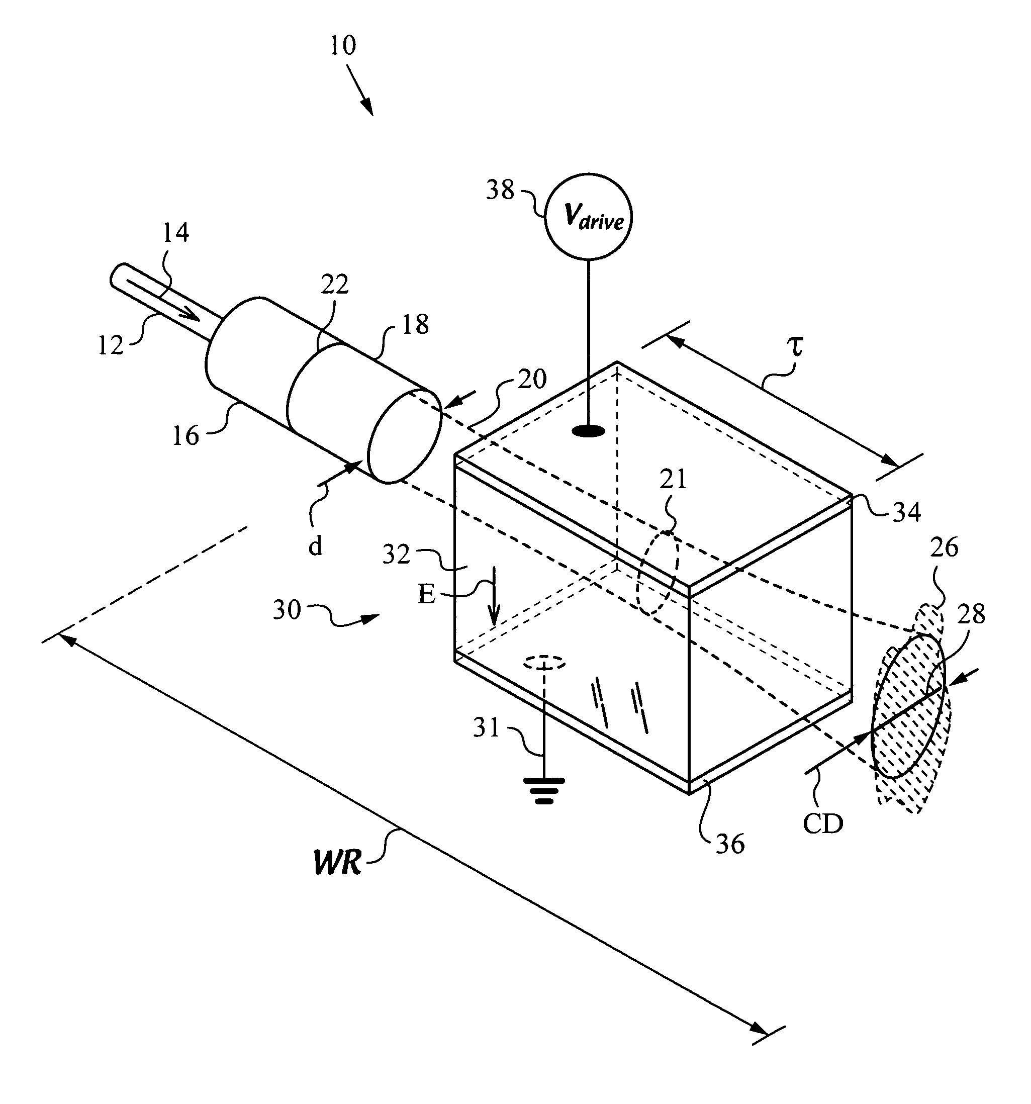
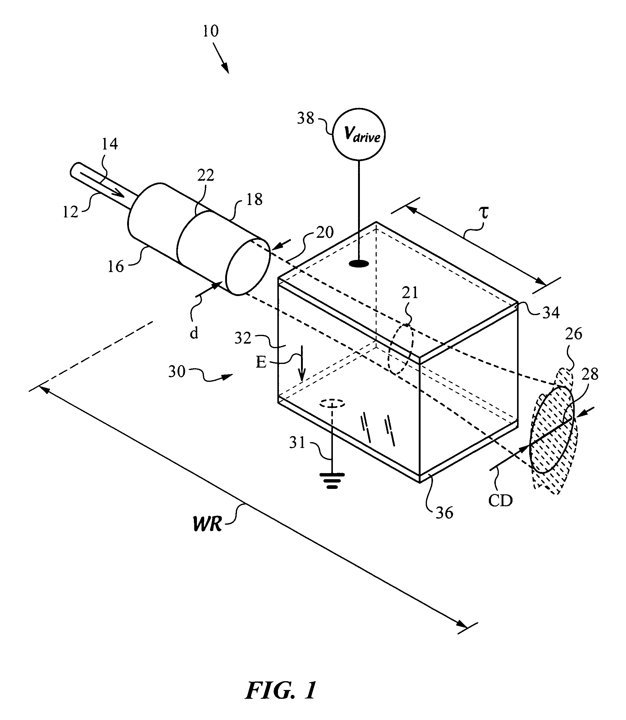
[0028]The present invention will be best understood by first reviewing the principles of the invention as illustrated in a portion of an electro-optic apparatus 10 shown in FIG. 1. Apparatus 10 is designed to interface with a fiber 12 that guides a light beam 14. Fiber 12 is received in a coupling unit or ferrule 16 that has a central bore (not shown) for retaining fiber 12. A person skilled in the art will recognize that ferrule 16 is only one of many possible ways of receiving a fiber and that other suitable ways and devices can be used for this purpose.

[0029]Apparatus 10 has a lens 18 for collimating light beam 14 to a collimated beam 20. Lens 18 is a graded index (GRIN) lens or preferably a curved surface lens or C-lens. To ensure good optical coupling between fiber 12 and lens 18, an interface 22 between ferrule 16 and lens 18 should be polished at an angle of a few degrees. This is just one of the methods that a person skilled in the art will be familiar with, and it should be...


PUM

PropertyMeasurementUnit
diameteraaaaaaaaaa
drive voltageaaaaaaaaaa
thicknessaaaaaaaaaa

Abstract

An apparatus and method to operate on a light beam by using a lens that collimates the light beam to a collimated beam with at least one cross-sectional dimension less than a critical dimension of 400 μm or less over a working range WR. The apparatus has a bulk electro-optic material of small thickness τ, e.g., less than 300 μm positioned within working range WR and the collimated beam traverses it along its path. The apparatus has a voltage source for applying a low operating or drive voltage Vdrive, e.g. less than 400 V to the bulk electro-optic material for performing an operation on the collimated beam. The lens for collimating the light beam is a free-space collimator such as a graded index (GRIN) lens or preferably a C-lens. The apparatus is a versatile and scalable platform that can be employed in building various electro-optic devices.

Description

RELATED APPLICATIONS[0001]This patent application claims priority to U.S. Provisional Patent applications 60 / 680,468 filed on May 11, 2005 and 60 / 681,050 filed on May 16, 2005, which are hereby incorporated by reference.FIELD OF THE INVENTION[0002]This invention relates generally to reconfigurable optical devices such as switches, variable splitters, variable attenuators and other devices in which port-to-port coupling properties are controlled.BACKGROUND ART[0003]Electrically reconfigurable optic devices direct optical signals along selected fibers, or control optical signal intensity within a fiber link, or select wavelength band of an optic network in which light signals are transmitted along optical fibers to transfer information from one location to another. Optical devices of this type should have the following performance characteristics: high speed operation, low optical insertion loss, high reliability, low power consumption, easy to drive, and low cost to produce. Although...

Claims


Application Information

Patent Timeline
Patent Type & Authority Patents(United States)
IPC IPC(8): G02B6/26G02B6/32G02F1/03
CPCG02B6/32G02F1/0311G02F2203/48G02F1/31
Inventor ZHAO, JINGGUANGHAI, JINYONGJUN, SHU
Owner AGILTRON
Why Eureka
Try Eureka