Bolometric detector, device for detecting infrared radiation using such a detector and method for producing this detector

a detector and detector technology, applied in radiation pyrometry, instruments, material analysis, etc., can solve the problems of increasing electrical noise, occurrence of areas where the current density exceeds the average density, and unsuitable for the readout circuit of every resistance value, so as to achieve the maximum useful surface area of bolometric material

Inactive Publication Date: 2008-07-29
ULIS SAS
View PDF6 Cites 4 Cited by
  • Summary
  • Abstract
  • Description
  • Claims
  • Application Information

AI Technical Summary

Benefits of technology

[0060]The object of the present invention is to maximise the useful surface area of the bolometric material (maximise the product W.L) regardless of the resistivity of the bolometric material without the resulting performance of the detector being affected by excess noise associated, in particular, with point effects that are inherent to an interdigitated configuration of electrodes or conductive parts (5).
[0072]This being so, the inactive surface areas of the detector according to the invention are reduced significantly in favour of useful surface areas whilst at the same time diminishing the excess noise associated with constriction of current flows which varies depending on the detailed configuration of the conductor elements and the bolometric material used.

Problems solved by technology

In fact, one of the difficulties encountered by those skilled in the art when defining bolometer structures is that of obtaining an electrical resistance R of an adequate value at around ambient temperature between the two conductive parts or electrodes (5) across which the driving voltage is applied.
Designing a bolometric detector shows that every resistance value is unsuitable for the readout circuit used by the designer of the product.
The drawback associated with the structure that uses interdigitated electrodes, as shown in FIG. 1, is the occurrence of areas where the current density exceeds the average density on the internal ends of conductive parts (5) as a result of the “point effect”.
These electric current concentrations result in an increased electrical noise level which is harmful to high detector performance.
However, in this configuration, roughly half the surface of the membrane cannot be used to optimise current flows because optimising infrared absorption demands substantially uniform distribution of conductive parts (5) over the surface of the membrane.
However, this result is obtained at the expense of not insignificant additional fabrication complexity and also complicates the problem of excess noise that is inherent in the point effect if it proves necessary to use interdigitated electrodes.
It is therefore apparent that, in both the above-mentioned documents according to the prior art, the absorber is produced by means of the same layer of material as the current supply electrodes, with all the advantages associated with this layout, but also the drawback described above of difficulty in obtaining an electrical resistance that is well-suited to the readout circuit.
Its implementation is, therefore, extremely complex.
In addition, the technology defined in this document naturally optimises current flows and therefore the low-frequency noise level since one is in a situation where the electrodes are placed far apart at two opposite edges of the elementary detector, on the other hand, this particular layout is only applicable to materials having a very low resistivity, typically vanadium oxides, otherwise the electrical resistance of the membrane is too high to obtain correct driving by the readout circuit and, in practice, it cannot be applied to amorphous silicon and similar materials.

Method used


Image

  • Bolometric detector, device for detecting infrared radiation using such a detector and method for producing this detector
  • Bolometric detector, device for detecting infrared radiation using such a detector and method for producing this detector
  • Bolometric detector, device for detecting infrared radiation using such a detector and method for producing this detector

Examples


Embodiment Construction

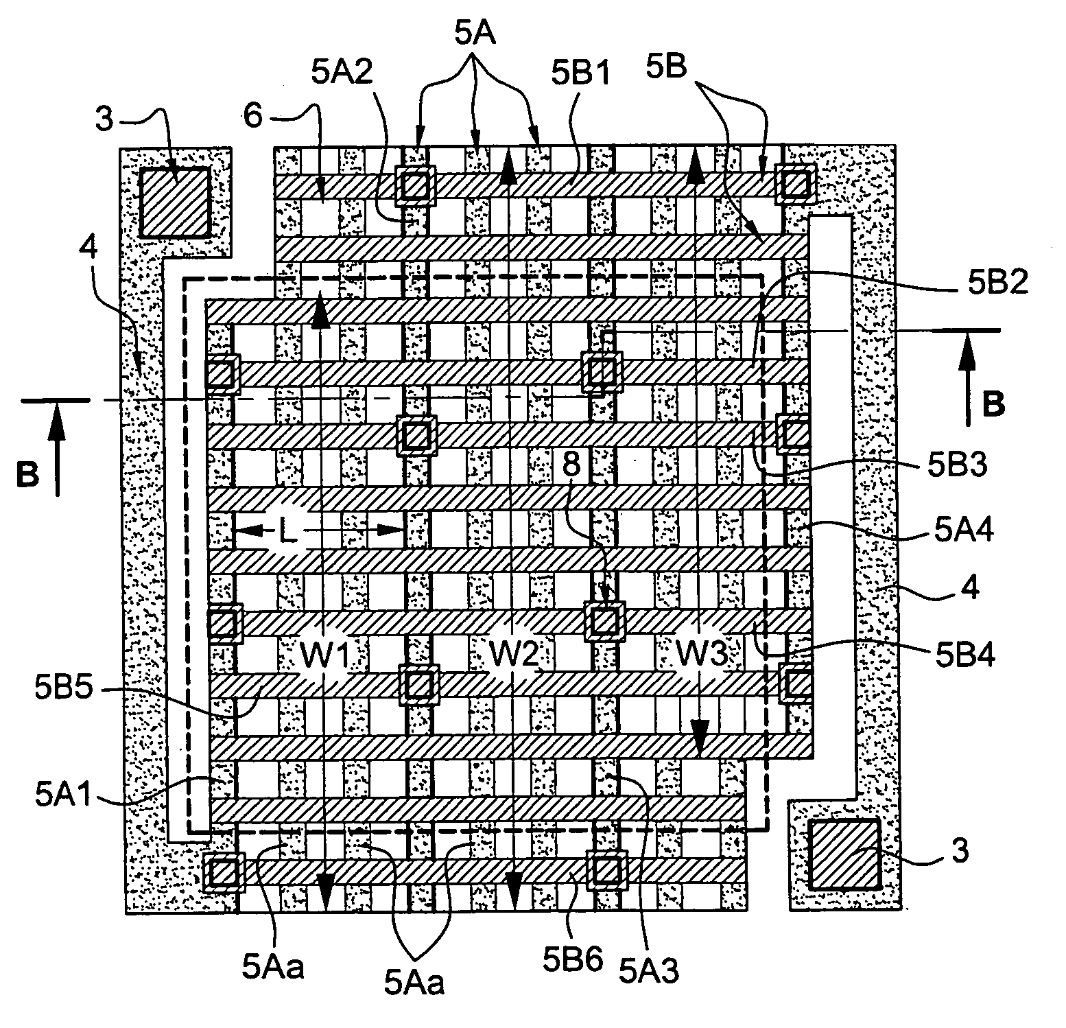
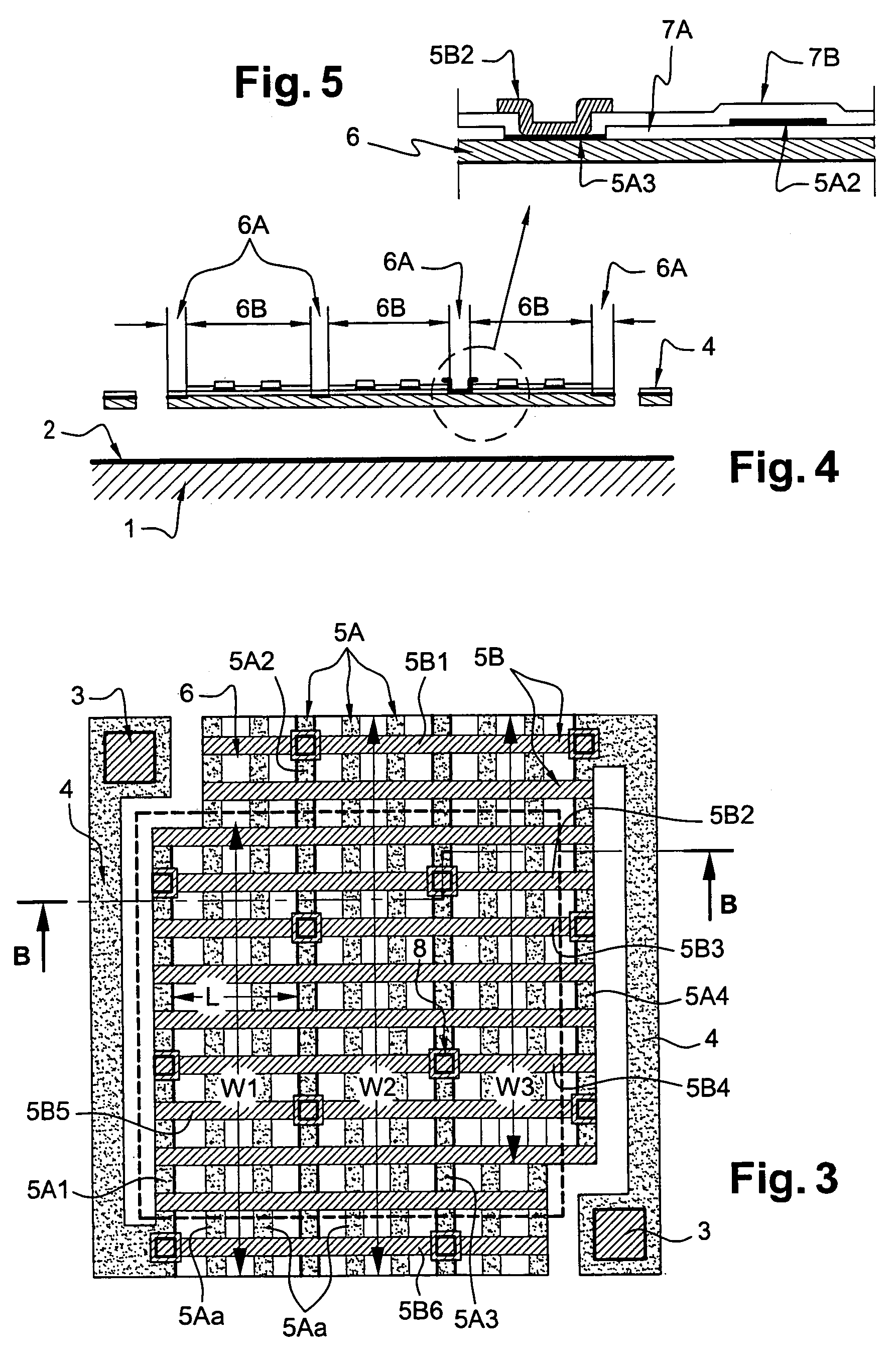
[0083]The invention therefore initially relates to an elementary bolometric detector and, more particularly, the configuration and layout of the conductive tracks on its sensitive part which itself constitutes the heart of the membrane. These conductive tracks function, as appropriate, as electrodes, i.e. they supply electric current from the readout circuit to the sensitive part, and as an absorber of the infrared radiation to be detected, or only function as an absorber.

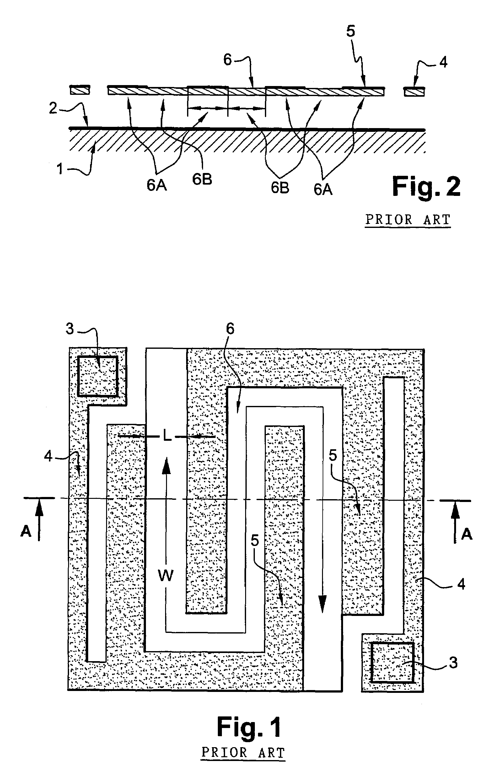
[0084]FIG. 3 shows a typical embodiment of the bolometric membrane according to the invention. The various components that are also common to FIG. 1 have the same reference numeral.

[0085]According to a fundamental feature of the invention, said membrane accommodates two separate networks of conductive tracks (5).

[0086]The first network consists of a series of conductive tracks (5A) that are essentially straight and parallel to each other. In the example described, four of these tracks (5A1, 5A2, 5A3 and 5A4) are in...


PUM


Abstract

A bolometric detector for electromagnetic radiation comprising a sensitive part or membrane comprising one or more layers of a sensitive material, the resistivity of which varies with temperature; first electric conductor elements in electrical continuity with a readout circuit associated with the bolometric detector and acting as electrodes for the detector and being in contact with the sensitive material and acting as an electromagnetic radiation absorber; second electric conductor elements at a floating potential acting only as an electromagnetic radiation absorber; at least one support area for the sensitive part fulfilling the function of positioning the sensitive part and electric conductor in relation to the readout circuit; at least one thermal isolation structure electrically and mechanically linking each support area to the sensitive part. The conductor elements are distributed as two crossed, superimposed networks of conductive tracks, the first of the two networks comprising all the first conductor elements.

Description

FIELD OF INVENTION[0001]The present invention relates to a bolometric detector and to a device for detecting infrared radiation using such a detector. It also relates to a method for producing such a detector. The invention has applications in the field of infrared imaging in particular.DESCRIPTION OF THE PRIOR ART[0002]In the area of infrared detectors, devices configured in the form of an array and capable of operating at ambient temperature, i.e. not requiring cooling to extremely low temperatures, are known—in contrast to detecting devices called “quantum detectors” which can only operate at extremely low temperature, typically that of liquid nitrogen.[0003]These uncooled detectors traditionally use the variation in a physical unit of an appropriate material as a function of temperature at around 300 K. In the case of bolometric detectors, this physical unit is electrical resistivity.[0004]Such an uncooled detector generally includes:[0005]means of absorbing the infrared radiati...

Claims


Application Information

Patent Timeline
Patent Type & Authority Patents(United States)
IPC IPC(8): G01J5/00
CPCG01J5/20
Inventor VILAIN, MICHEL
Owner ULIS SAS
Why Eureka
Try Eureka