Shift register

a technology of shift register and register, applied in the field of shift register, can solve the problems of drive errors, significant shift in the threshold voltage vth of the transistor, inferior electrical characteristics of the polycrystalline silicon thin-film transistor, etc., and achieve the effect of removing the shift in the threshold voltage of the transistor

Active Publication Date: 2008-07-29
WINTEK CORP
View PDF16 Cites 15 Cited by
  • Summary
  • Abstract
  • Description
  • Claims
  • Application Information

AI Technical Summary

Benefits of technology

[0014]Hence, an object of the invention is to provide a shift register capable of eliminating the shift in the threshold voltage of a transistor.
[0016]Through the design of the invention, when the threshold voltage of the first or the second transistor is increased, the voltage of the second node is also increased with the same increment so as to maintain low on-resistances of the first and second transistors and improve the response speed of a switch between the first power voltage and the second power voltage. Accordingly, the bias voltage of the transistors in the unit stage can be dynamically adjusted to avoid harmful fluctuations in the threshold voltage, thus improving the stability of a shift register and extending the lifespan of a display panel.

Problems solved by technology

An amorphous silicon thin-film transistor is often used in an active matrix type LCD due to its low fabrication cost and high production yield; however, some of its electrical characteristics are inferior compared with a polycrystalline silicon thin-film transistor.
Therefore, since the NMOS transistors Q2 and Q4 are always positively biased for a long time, they are liable to malfunction to result in a considerable shift in the threshold voltage Vth of a transistor.
This may cause the gate drive circuit to transmit distorted scan signals to result in drive errors.
Under the circumstance, the gate drive circuit may transmit distorted scan signals to result in drive errors that worsen the display quality of a display panel.
However, the first NMOS transistor M2a may relieve the shift in the threshold voltage only at the moment the output signal OUTi is pulled down, but, at the remaining moments, the shift in the threshold voltage of the NMOS transistor M2b still influences the operation of the unit stage 21 to result in drive errors.

Method used


Image

  • Shift register
  • Shift register
  • Shift register

Examples


Embodiment Construction

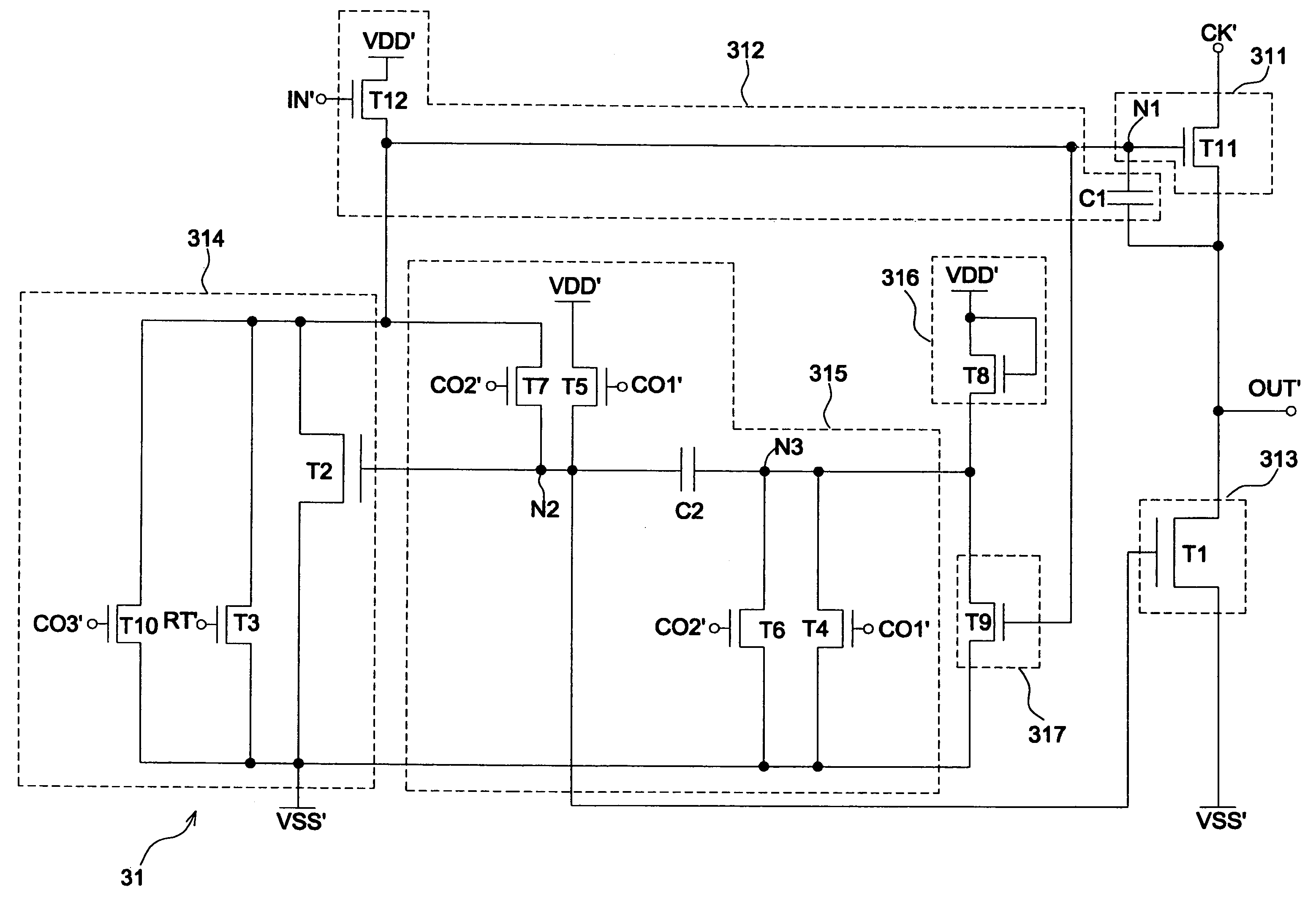
[0027]FIG. 3A shows a schematic diagram illustrating a shift register 30 according to an embodiment of the invention. The shift register 30 is provided in a gate drive circuit constructed by amorphous silicon thin film transistors (a-Si TFTs).

[0028]The shift register 30 includes N (N is a positive integer) number of unit stages 311-31N. Each unit stage 31 includes an input terminal IN′, an output terminal OUT′, a feedback control terminal RT′, a clock signal input terminal CK′, a first control signal input terminal CO1′, a second control signal input terminal CO2′, a third control signal input terminal CO3′, a first power voltage terminal VSS′, and a second power voltage terminal VDD′. The unit stages 311-31N are connected with one another in succession. The input terminal IN′ of a first unit stage 311 receives a threshold signal St as an input signal IN for driving the unit stage 311 to generate a first output signal OUT1. The input terminal IN′ of the Qth (Q is a positive integer;...


PUM


Abstract

A shift register includes multiple stages connected with each other in succession. The shift register stores the threshold voltage of an amorphous silicon thin-film transistor in a capacitor. During operation, the bias applied to the transistor is adjusted according to the threshold voltage stored in the capacitor.

Description

BACKGROUND OF THE INVENTION[0001](a) Field of the Invention[0002]The invention relates to a shift register, particularly to a shift register constructed by amorphous silicon thin-film transistors.[0003](b) Description of the Related Art[0004]Typically, thin-film transistor liquid crystal displays (TFT-LCDs) are divided into two types, the amorphous silicon TFT LCD (a-Si TFT-LCD) and the polycrystalline silicon TFT LCD (poly-Si TFT-LCD). An amorphous silicon thin-film transistor is often used in an active matrix type LCD due to its low fabrication cost and high production yield; however, some of its electrical characteristics are inferior compared with a polycrystalline silicon thin-film transistor. Thus, an amorphous silicon gate (ASG) technology accompanied by many testified circuit architectures is proposed to combine with the application of the amorphous silicon thin-film transistor, so that the amorphous silicon thin-film transistor may compare favorably with the polycrystalline...

Claims


Application Information

Patent Timeline
Patent Type & Authority Patents(United States)
IPC IPC(8): G11C19/00
CPCG11C19/28G09G3/36G09G3/3677G09G2300/0408G09G2310/0286G09G2330/06
Inventor LO, SHIN-TAIHSU, CHING-FULIAO, WEN-TUI
Owner WINTEK CORP
Why Eureka
Try Eureka