Vertical transistor structure for use in semiconductor device and method of forming the same

a technology of vertical transistors and semiconductor devices, which is applied in the direction of non-mechanical control, electric permutation locks, lock applications, etc., can solve the problems of difficulties and limitations of obtaining high-integrated semiconductor devices, and achieve the effect of reducing cell size and high-integrated semiconductor devices

Active Publication Date: 2008-08-05
SAMSUNG ELECTRONICS CO LTD
View PDF23 Cites 24 Cited by
  • Summary
  • Abstract
  • Description
  • Claims
  • Application Information

AI Technical Summary

Benefits of technology

[0011]Some embodiments of the invention provide a vertical transistor structure and a method for forming the same, in which a unit memory cell has a (4F2) structure. A gate electrode is formed in a vertical type, and a first contact connected to an upper bit line is formed between gate electrodes. In both sides of the gate electrode a second contact connected to a storage node is formed. Hence, unit memory cells constituting a semiconductor device have a (4F2) structure, reducing a cell size and providing high-integrated semiconductor devices.

Problems solved by technology

Hence, obtaining a highly-integrated semiconductor device has difficulties and limitations, in particular to integrate beyond a given level.

Method used


Image

  • Vertical transistor structure for use in semiconductor device and method of forming the same
  • Vertical transistor structure for use in semiconductor device and method of forming the same
  • Vertical transistor structure for use in semiconductor device and method of forming the same

Examples


Embodiment Construction

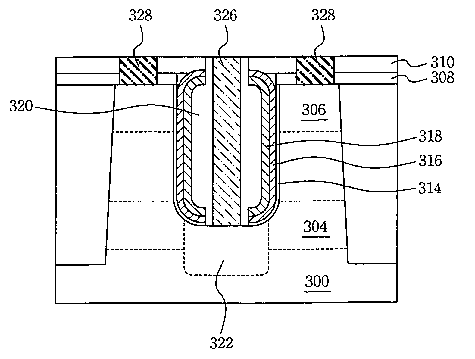
[0017]Exemplary embodiments of the invention are more fully described in detail with reference to FIGS. 2 to 14. The invention may be embodied in many different forms and should not be construed as being limited to the exemplary embodiments set forth herein. Rather, these exemplary embodiments are provided so that this disclosure is thorough and complete, and to convey the concept of the invention to those skilled in the art.

[0018]FIG. 2 is a plan view illustrating a layout structure of a vertical transistor according to an exemplary embodiment of the invention.

[0019]Referring first to FIG. 2, two gate electrodes 230 distanced by a predetermined interval are disposed in parallel in a lengthwise direction of an active region within the active region surrounded by a non-active region 210. A first contact 260 connected to a bit line is formed in an active region between the gate electrodes 230, and a second contact 250 connected to a storage node is formed in an active region of both s...


PUM


Abstract

According to some embodiments, a structure of vertical transistor includes gate electrodes distanced by a predetermined interval in an active region, formed in a vertical shape to have a predetermined depth from a top surface of a semiconductor substrate. A gate insulation layer is formed between one side wall of the gate electrode and the substrate. A gate spacer is formed in another sidewall of the gate electrode, covering the gate electrode. A contact plug is formed between the gate spacer. A plug impurity layer is formed in a lower part of the contact plug, and source and drain are formed opposite to the gate electrode within the active region. Thereby, an area occupied by a gate electrode is substantially reduced, so a unit memory cell has a 4F2 structure, reducing a memory cell size, by forming a vertical-type gate electrode within an active region.

Description

CROSS REFERENCE TO RELATED APPLICATIONS[0001]This application claims priority from Korean Patent Application No. 2004-12486, filed on Feb. 25, 2004, the contents of which are hereby incorporated by reference for all purposes.BACKGROUND OF THE INVENTION[0002]1. Field of the Invention[0003]This disclosure relates to semiconductor devices, and more particularly, to a vertical transistor structure having a vertical-type gate and to a method of forming the same.[0004]2. Description of the Related Art[0005]Requirements for semiconductor devices with lower electricity consumption and higher capacitance have prompted researchers to develop higher integrated and higher speed semiconductor devices. In particular, a semiconductor memory cell, a DRAM (Dynamic Random Access Memory), has been used widely, and research is focused on ways to enhance the speed and integration of this device.[0006]In general, a DRAM is constructed of one MOS (Metal Oxide Semiconductor) transistor and one storage capa...

Claims


Application Information

Patent Timeline
Patent Type & Authority Patents(United States)
IPC IPC(8): H01L29/739H01L21/336H01L21/8242H01L27/108H01L29/78H01L29/94
CPCH01L27/10876H01L27/10888H01L29/7827H01L29/66666H01L27/10891H01L27/10855H01L29/66621H10B12/0335H10B12/053H10B12/488H10B12/485E05B49/00E05B65/0025E05B9/02E05B2047/0087
Inventor KIM, JI-YOUNG
Owner SAMSUNG ELECTRONICS CO LTD
Why Eureka
Try Eureka