Low power preamplifier writer architecture

a preamplifier and writer technology, applied in the direction of pulse technique, motor/generator/converter stopper, dynamo-electric converter control, etc., can solve the problem of relatively high power consumption of the driver circuit b>100/b>

Active Publication Date: 2008-08-05
MARVELL ASIA PTE LTD
View PDF9 Cites 20 Cited by
  • Summary
  • Abstract
  • Description
  • Claims
  • Application Information

AI Technical Summary

Benefits of technology

[0021]Such embodiments may further include code for inhibiting junction diodes of transistors used to sink current to the ground terminal from conducting current during the boost cycle. The current received by the first node may have the same level as the current received by the second node and the first and second resistors may have the same resistance. Such embodiments may further include code for supplying a third current

Problems solved by technology

Consequently, driver circuit 100 has a relatively hi

Method used


Image

  • Low power preamplifier writer architecture
  • Low power preamplifier writer architecture
  • Low power preamplifier writer architecture

Examples


exemplary embodiment 250

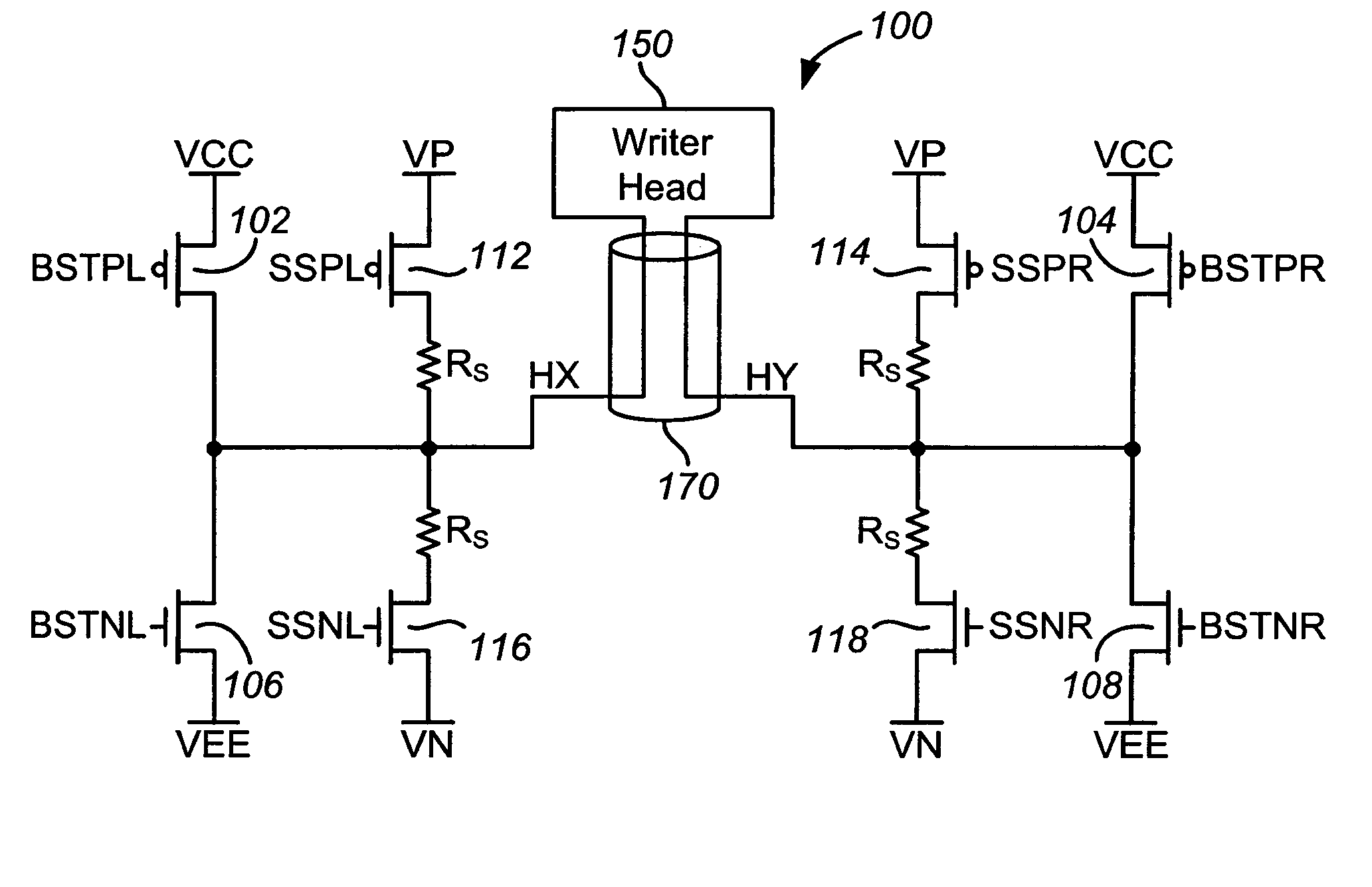
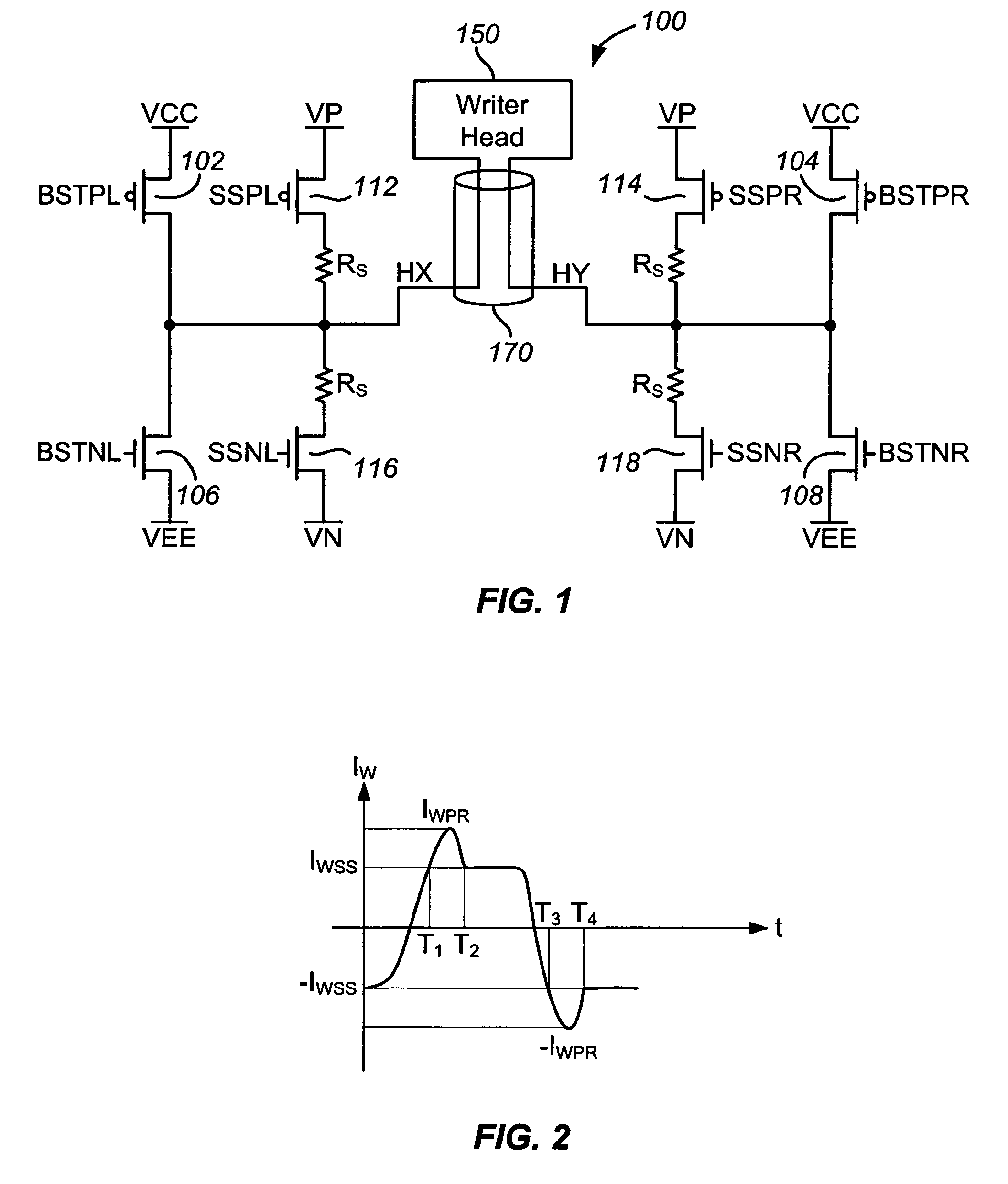
[0031]Driver circuit 200 is also shown as including, in part, a switch circuit 250 that is disposed between nodes Hx and Hy, and when activated, provides a current path between these two nodes. Exemplary embodiment 250 of this switch circuit is shown as including resistors 252, 254, NMOS transistors 256, 258 and PMOS transistor 260. Resistor 252 has a first terminal coupled to node Hx, and a second terminal coupled to one of the current carrying terminals of NMOS transistor 256. Resistor 254 has a first terminal coupled to node Hy, and a second terminal coupled to one of the current carrying terminals of NMOS transistor 258. The second current carrying terminal of transistor 256 is coupled to a first current carrying terminal of PMOS transistor 260 whose second current carrying terminal is coupled to the second current carrying terminal of transistor 258. Nodes Hx and Hy see a balanced load due to the symmetry provided by resistors 252, 254, as well as transistors 256, 258, 260 disp...

exemplary embodiment 200

[0038]As seen from expression (4), during the steady state periods, the current consumption of exemplary embodiment 200 of the present invention, does not depend on any negative supply voltage. This is in contrast to the prior art driver circuit 100 shown in FIG. 1, whose current consumption during the steady state periods depends both on the positive supply voltage VCC as well as the negative supply voltage VEE. Accordingly, driver circuit 200 of the present invention has a reduced current consumption relative to the prior art driver circuits.

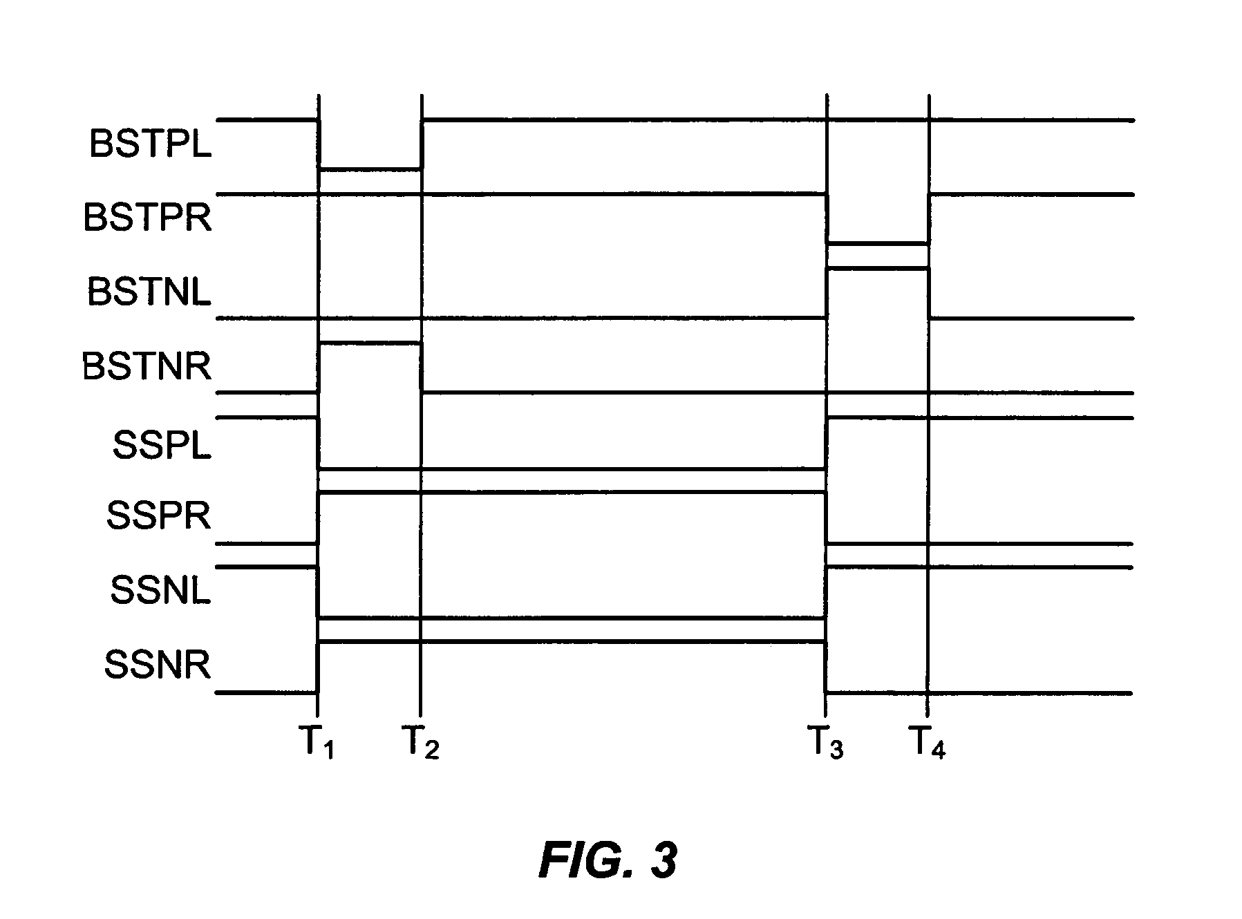
[0039]FIG. 5 is a timing diagram of a number of signals associated with driver circuit 200. During the first boost period TB1, voltage signal BSTPL is lowered, voltage signal BSTNL is maintained low, voltage signal BSTPR is maintained high and voltage signal BSTNR is raised to a high level. Accordingly, transistors 202, 208 are turned on and transistors 204, 206 are turned off or maintained off. Therefore, a current path is established from su...


PUM


Abstract

A circuit is adapted to activate a writer head of a data storage media drive during both the boost periods as well as the steady state periods. The current supplied to the writer head during the boost periods exceeds the steady state current and flows between positive and negative voltage supplies so as to provide the required magnetic flux change in the inductor disposed in the write head. During the steady state periods, a switch circuit is turned on to provide a second current path across the writer head. During the steady state periods, the current flows between the positive voltage supply and the ground to reduce power consumption. The switch circuit is turned off during the boost periods.

Description

CROSS-REFERENCES TO RELATED APPLICATIONS[0001]The present application claims benefit under 35 USC 119(e) of the following applications, the contents of all of which is incorporated herein by reference in their entirety:U.S. provisional application No. 60 / 710,898, filed Aug. 23, 2005, entitled “Low Power Preamplifier Writer Architecture”;U.S. provisional application No. 60 / 717,725, filed Sep. 15, 2005, entitled “Low Power Preamplifier Writer Architecture”;U.S. provisional application No. 60 / 710,796, filed Aug. 23, 2005, entitled “Switch Circuit”.BACKGROUND OF THE INVENTION[0002]The present invention relates to electronic circuits, and more particularly to a technique for reducing power consumption of a writer head driver circuitry disposed in a data storage media driver.[0003]FIG. 1 is a simplified transistor schematic diagram of a driver circuit 100 used to supply current to a writer head 150 via nodes Hx and Hy. FIG. 2 shows the timing characteristic of the write current Iw so supp...

Claims


Application Information

Patent Timeline
IPC IPC(8): H02P3/00H03K3/00
CPCG11B5/09G11B5/022
Inventor KONG, CHAN SANGTAN, KIEN BENGMIAO, XIAO YU
Owner MARVELL ASIA PTE LTD
Why Eureka
Try Eureka