Non-linearity compensation circuit and bandgap reference circuit using the same

a non-linearity compensation and reference circuit technology, applied in the direction of power supply lines, instruments, vehicle components, etc., can solve the problems of limited compensation effect of reference voltage vsub>bg1 /sub>, non-linearity effect still exists, non-linearity effect, etc., to improve the precision of reference voltage and low circuit cost of non-linearity compensation circuits

Inactive Publication Date: 2008-08-12
FARADAY TECH CORP
View PDF16 Cites 44 Cited by
  • Summary
  • Abstract
  • Description
  • Claims
  • Application Information

AI Technical Summary

Benefits of technology

[0020]Another objective of the present invention is to provide a non-linearity compensation circuit and a bandgap reference circuit using the same, wherein the non-linearity compensation circuit can improve the precision of the reference voltage.
[0021]Still another objective of the present invention is to provide a non-linearity compensation circuit and a bandgap reference circuit using the same, wherein the circuit cost of the non-linearity compensation circuit is low, so it can be applied widely.

Problems solved by technology

Therefore, the compensation effect of the reference voltage VBG1 is limited, and the non-linearity effect still exists.
However, in the conventional bandgap reference circuit, VBE has a non-linearity effect.
Thus, the actual reference voltage exhibits quite a large difference in operating temperature range.

Method used


Image

  • Non-linearity compensation circuit and bandgap reference circuit using the same
  • Non-linearity compensation circuit and bandgap reference circuit using the same
  • Non-linearity compensation circuit and bandgap reference circuit using the same

Examples


first embodiment

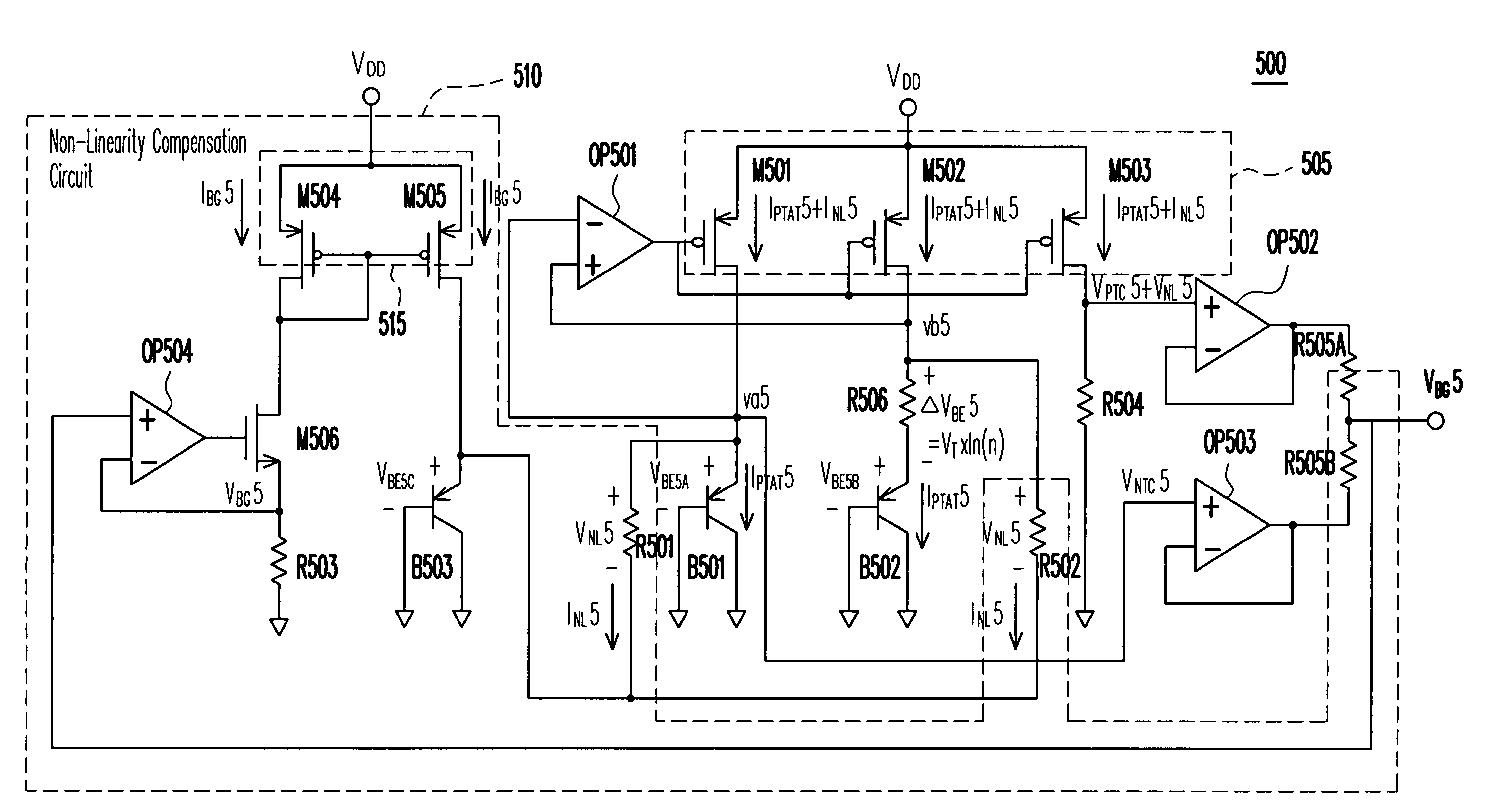
[0036]FIG. 5 is a circuit diagram of a bandgap reference circuit according to the present invention. The bandgap reference circuit 500 of this embodiment at least comprises a PTAT current mirror 505 formed by MOS transistors M501˜M503, operation amplifiers OP501˜503, BJT transistors B501 and B502, resistors R504, R505A, R505B and R506, and a non-linearity compensation circuit 510. The non-linearity compensation circuit 510 at least includes a temperature independent current mirror 515 formed by MOS transistors M504 and M505, an operation amplifier OP504, an MOS transistor M506, a BJT transistor B503, and resistors R501, R502, and R503.

[0037]The source of the MOS transistor M501 is connected to a power source VDD, the drain thereof is connected to the emitter of the BJT transistor B501 (i.e., node Va5), and the gate thereof is connected to the output of the operation amplifier OP501 and the gates of the MOS transistors M502 and M503. The source of the MOS transistor M502 is connected...

second embodiment

[0065]FIG. 9 is a circuit diagram of a bandgap reference circuit 500′ according to the present invention. The architecture of the bandgap reference circuits 500′ is similar to that of the bandgap reference circuit 500 shown in FIG. 5, so the same or like reference symbols represent the same or like elements, only except that the operation amplifiers OP502, OP503 and the resistor R504 in FIG. 5 are replaced by the BJT transistor B504′ and the resistor R504′ in FIG. 9.

[0066]With the concept of FIG. 5, it can be known that the reference voltage VBG5′ generated by the architecture of FIG. 9 can be represented by the following equation:

[0067]VBG⁢⁢5′=⁢VNTC′+VPTC′+VNL′=⁢[VBE⁢⁢5⁢D+R⁢⁢504′·(Δ⁢⁢VBE⁢⁢5′R⁢⁢506′+VNL⁢⁢5′R⁢⁢502′)]=⁢{[VBG⁢5′-(VBG⁢5′-VBE⁢⁢0)⁢TT0-(η-1)⁢VT⁢ln⁢TT0]+⁢[R⁢⁢504′R⁢⁢506′·VT·ln⁡(n)]+⁢[R⁢⁢504′R⁢⁢502′⁢VT⁢ln⁢TT0]}(15)

[0068]In FIG. 9, the elements the same as or similar to the elements in FIG. 5 are represented with similar symbols. As the operation of the bandgap reference circu...


PUM


Abstract

A non-linearity compensation circuit and a bandgap reference circuit using the same for compensating non-linear effects of a reference voltage are provided. In the non-linearity compensation circuit, the reference voltage is transformed into a temperature independent current. A current mirror mirrors the temperature independent current for biasing a bipolar junction transistor (BJT). Further, two resistors are used for estimating a non-linear voltage, so as to compensate the reference voltage.

Description

BACKGROUND OF THE INVENTION[0001]1. Field of Invention[0002]The present invention relates to a non-linearity compensation circuit and a bandgap reference circuit using the same, and more particularly, to a non-linearity compensation circuit capable of improving the precision of a bandgap reference voltage and a bandgap reference circuit using the same.[0003]2. Description of Related Art[0004]Digital-to-analog converters (DACs), analog-to-digital converters (ADCs) or regulators need at least one fixed and stable reference voltage. It is preferred that the reference voltage is stably regenerated each time the power source is started. An ideal reference voltage even had better not be influenced by processing differences, changes in the operating temperature, and power source variations.[0005]A bandgap reference circuit can be used to provide the reference voltage. Therefore, bandgap reference circuits play an important role in many electronic systems as they may determine the stability...

Claims


Application Information

Patent Timeline
Patent Type & Authority Patents(United States)
IPC IPC(8): G05F3/16
CPCG05F3/30Y10S323/907
Inventor CHANG, KUEN-SHANUANG, UEI-SHAN
Owner FARADAY TECH CORP
Why Eureka
Try Eureka