Acoustic mirror structure for a bulk acoustic wave structure and method for fabricating same

a bulk acoustic wave and mirror technology, applied in piezoelectric/electrostrictive/magnetostrictive devices, piezoelectric/electrostriction/magnetostriction machines, impedence networks, etc., can solve the problem of imposing or worsening undesired rf, relative low resistivity, and undesirable increase in electrical loss in bulk acoustic wave structures. problems, to achieve the effect of reducing electrical loss and increasing

Inactive Publication Date: 2008-08-19
AVAGO TECH WIRELESS IP SINGAPORE PTE
View PDF9 Cites 9 Cited by
  • Summary
  • Abstract
  • Description
  • Claims
  • Application Information

AI Technical Summary

Problems solved by technology

However, high density metal such as tungsten also have relatively low resistivity, which can impose or worsen undesired RF parasitic paths detrimental to device function including stray capacitances and image currents in the high acoustic impedance layers of the acoustic mirror structure due to its close proximity to the device's signal path.
These induced parasitics can cause an undesirable increase in electrical loss in the bulk acoustic wave structure.
Additional loss in bulk acoustic wave structures can be caused by scattering of acoustic waves at non-smooth interfaces between the layers of the structure, and acoustic viscosity seen by the waves traveling through the layers.
As a result, conventional acoustic wave structures that use insulators in high acoustic impedance layers typically require more additional low and high acoustic impedance layers to achieve a desired level of acoustic reflectivity, which undesirably increases manufacturing cost.
It is also the case that non-optimal choices for high and low impedance layer materials will reduce the observed electromechanical coupling of the bulk acoustic wave structures and as such reduce the bandwidth of filters in which they are used.

Method used


Image

  • Acoustic mirror structure for a bulk acoustic wave structure and method for fabricating same
  • Acoustic mirror structure for a bulk acoustic wave structure and method for fabricating same
  • Acoustic mirror structure for a bulk acoustic wave structure and method for fabricating same

Examples


Embodiment Construction

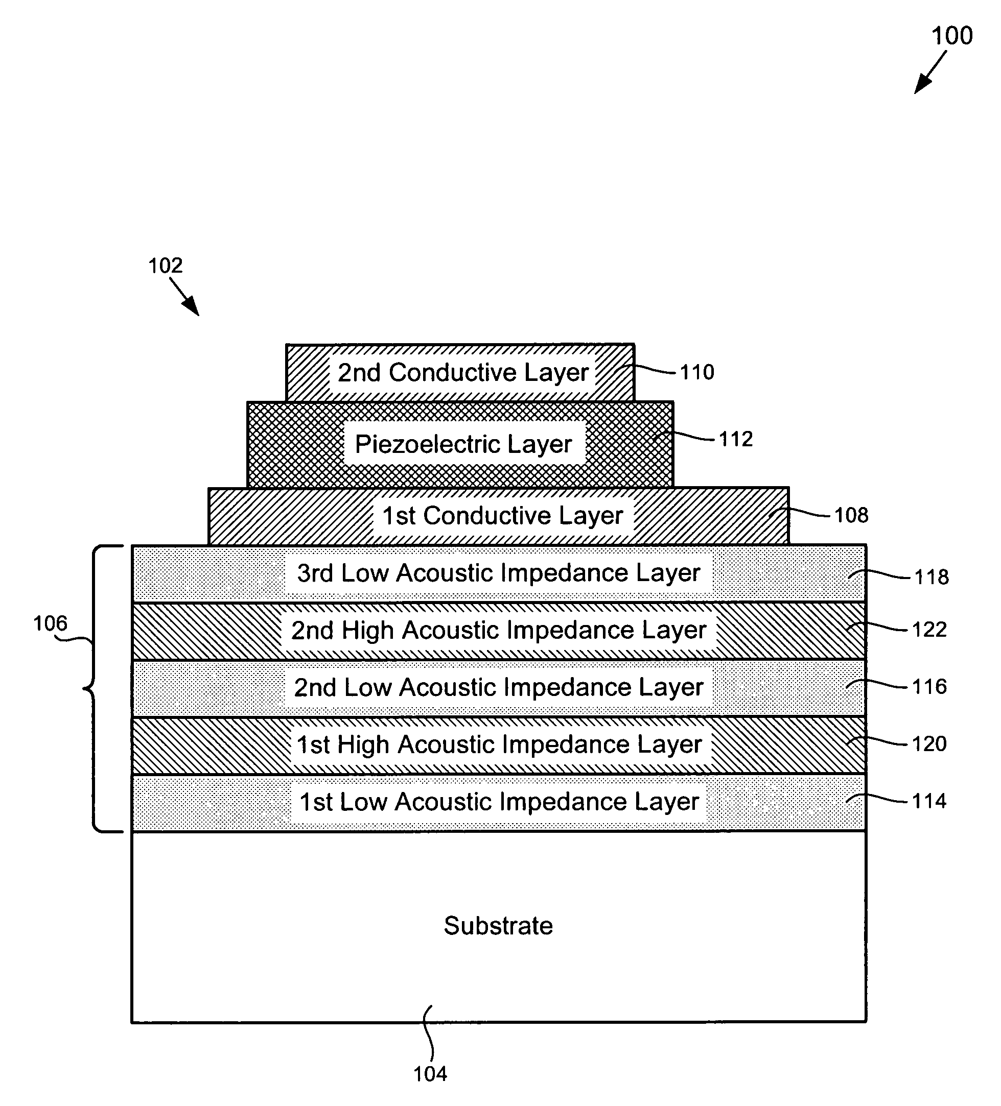
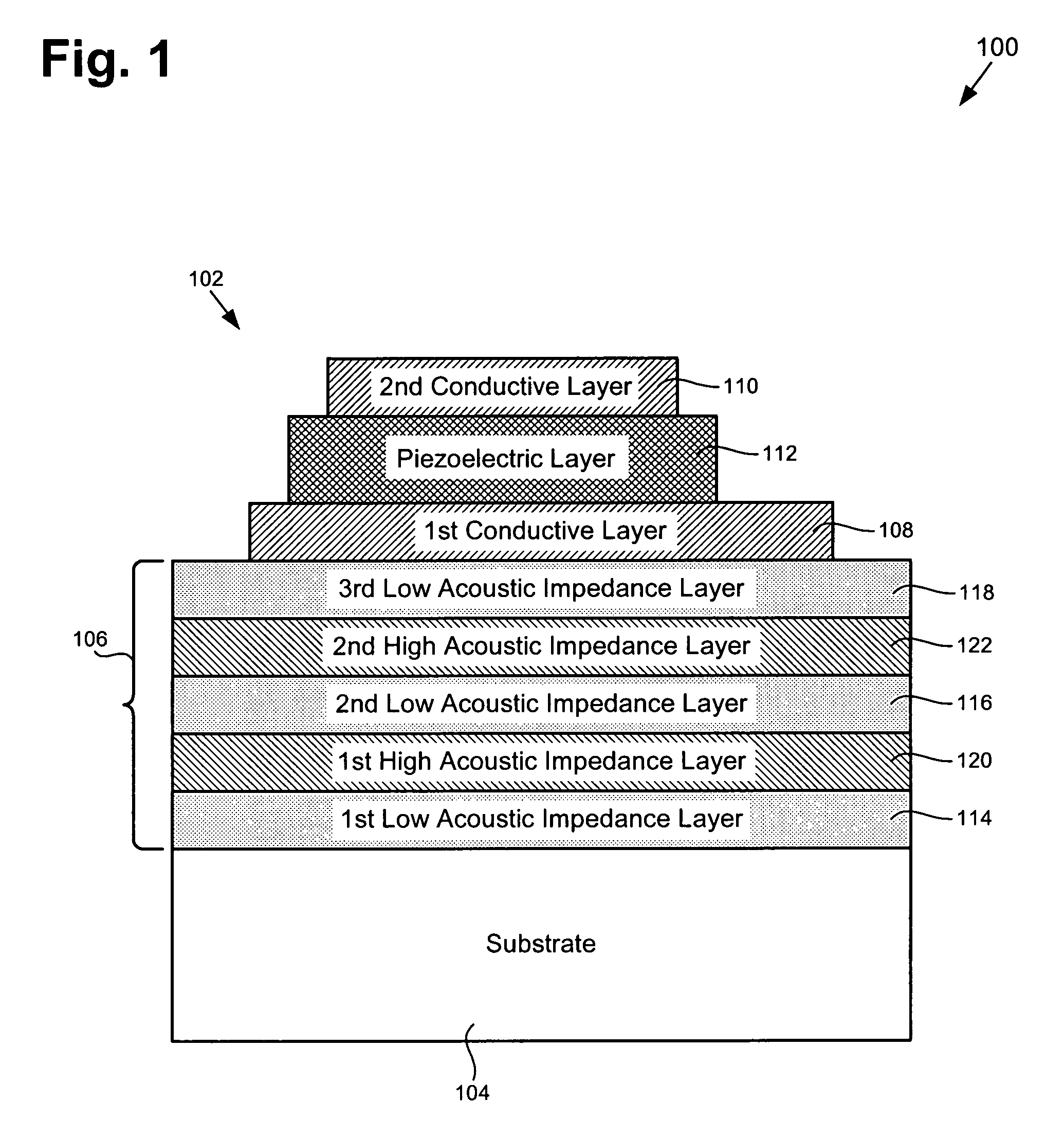
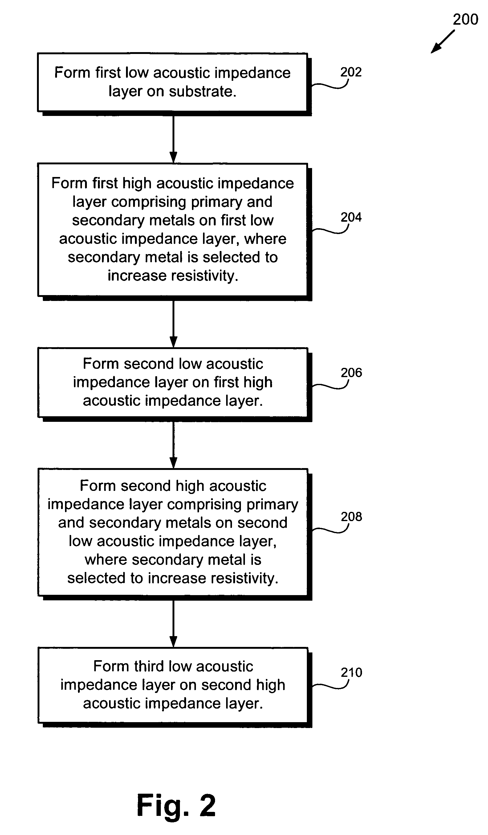
[0014]The present invention is directed to an acoustic mirror structure for a bulk acoustic wave structure and method for fabricating same. Although the invention is described with respect to specific embodiments, the principles of the invention, as defined by the claims appended herein, can obviously be applied beyond the specifically described embodiments of the invention described herein. Moreover, in the description of the present invention, certain details have been left out in order to not obscure the inventive aspects of the invention. The details left out are within the knowledge of a person of ordinary skill in the art.

[0015]The drawings in the present application and their accompanying detailed description are directed to merely exemplary embodiments of the invention. To maintain brevity, other embodiments of the invention which use the principles of the present invention are not specifically described in the present application and are not specifically illustrated by the ...


PUM

PropertyMeasurementUnit
thicknessaaaaaaaaaa
thicknessaaaaaaaaaa
acoustic wave structureaaaaaaaaaa

Abstract

According to one embodiment of the invention, an acoustic mirror structure situated in a bulk acoustic wave structure includes a number of alternating low acoustic impedance and high acoustic impedance layers situated on a substrate. Each high acoustic impedance layer includes a first mole percent of a primary metal and a second mole percent of a secondary metal, where the first mole percent of the primary metal is greater than the second mole percent of the secondary metal, and where the secondary metal causes each high acoustic impedance layer to have increased resistivity. According to this exemplary embodiment, the second mole percent of the secondary metal can cause only a minimal decrease in density of each high acoustic impedance layer. The increased resistivity of each high acoustic impedance layer can cause a reduction in electrical loss in the bulk acoustic wave structure.

Description

BACKGROUND OF THE INVENTION[0001]1. Field of the Invention[0002]The present invention is generally in the field of semiconductor fabrication. More specifically, the invention is in the field of fabrication of bulk acoustic wave structures in semiconductor dies.[0003]2. Background Art[0004]Bulk acoustic wave structures, which can be used in frequency control or filtering applications, can include a piezoelectric layer and an acoustic mirror structure. The acoustic mirror structure, which can include a number of alternating low and high acoustic impedance layers, can be used to trap acoustic energy in the piezoelectric layer. In the acoustic mirror structure, the level of acoustic reflectivity at the interface between a low and a high acoustic impedance layer determines the number of alternating low and high acoustic impedance layers the acoustic mirror structure requires to achieve a desired level of acoustic reflectivity. By way of background, the level of acoustic reflectivity at a...

Claims


Application Information

Patent Timeline
Patent Type & Authority Patents(United States)
IPC IPC(8): H01L41/08
CPCH03H9/175Y10T29/42
Inventor BARBER, BRADLEYGEHLERT, PAUL P.KENCHAPPA, SAHANASHEPARD, CHRISTOPHER F.
Owner AVAGO TECH WIRELESS IP SINGAPORE PTE
Why Eureka
Try Eureka