
Method for wafer level stack die placement

a stack die and stacking technology, applied in the direction of electrical equipment, semiconductor devices, semiconductor/solid-state device details, etc., can solve the problems of low stacking efficiency, low stacking efficiency, time-consuming conventional stack die placement method, etc., and achieve the effect of increasing the number of units per hour and quickly completing the wafer level stack die placemen

Active Publication Date: 2008-08-26
ADVANCED SEMICON ENG INC
View PDF2 Cites 7 Cited by
  • Summary
  • Abstract
  • Description
  • Claims
  • Application Information

AI Technical Summary

Benefits of technology

The present invention provides a method for wafer level stack die placement, which involves attaching a wafer to a photosensitive adhesive tape and then selectively exposing the tape to form an adhesion-released portion. This allows the die of the wafer to be detached from the tape and fixed on a die carrier, resulting in a faster and more efficient process for wafer level stack die placement. Additionally, the invention allows for the simultaneous placement of multiple dice on different die carriers, reducing the time and speeding up the production cycle.

Problems solved by technology

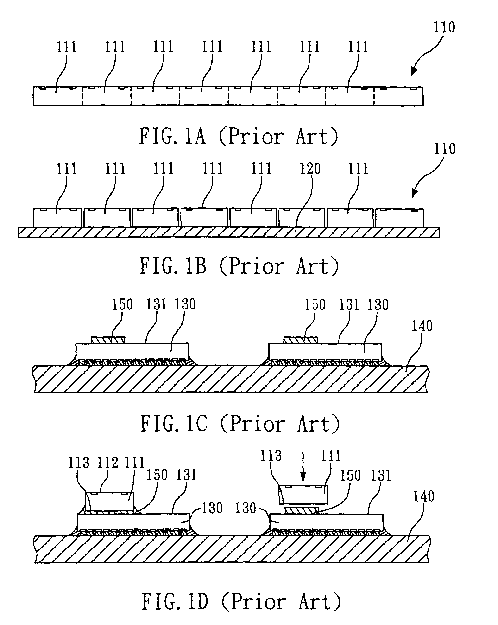
A conventional stacking way is picking and placing the individual die, which has a low efficiency in the stack die placement.
In the conventional method for stack die placement, the dice are picked and placed on the flip-chip dice 130 one by one by the pick & place arm after the wafer 110 is cut, so that the conventional method for stack die placement is time consuming and its stacking efficiency is rather low.

Method used


Image

  • Method for wafer level stack die placement
  • Method for wafer level stack die placement
  • Method for wafer level stack die placement

Examples


Embodiment Construction

[0014]The present invention will be illustrated in the following embodiments with reference to the accompanying drawings.

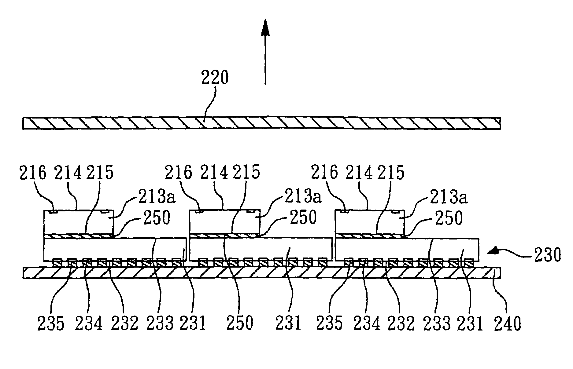
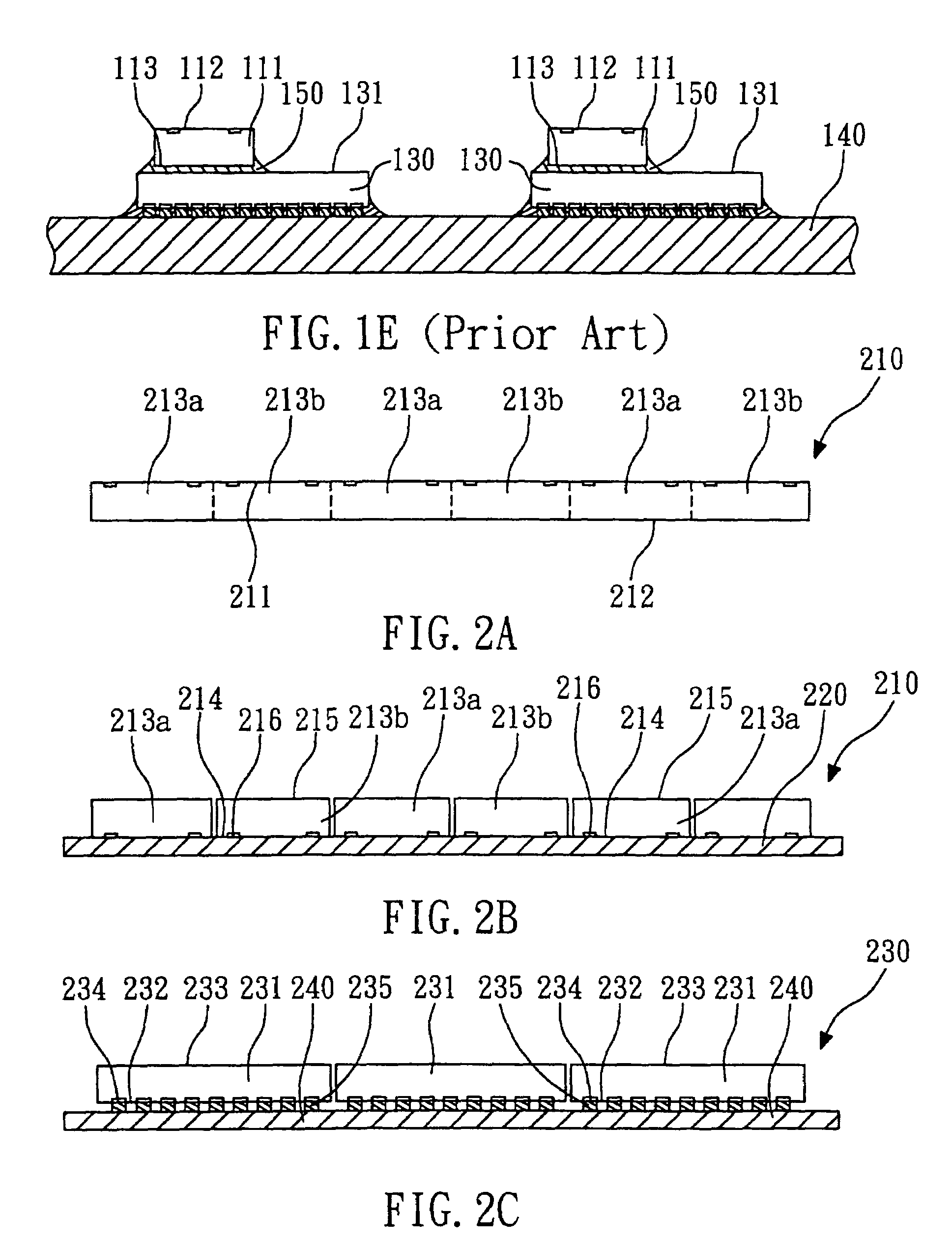
[0015]Referring to FIGS. 2A to 2K, a method according to an embodiment of the present invention is shown. Referring to FIG. 2A, a first wafer 210 is provided. The first wafer 210 has a first surface 211 and a corresponding second surface 212 and comprises a plurality of first dice. These first dice are divided into a plurality of die-attaching batches. In the present embodiment, these first dice of the first die-attaching batch are represented by the numeral 213a, and the first dice of the second die-attaching batch are represented by the numeral 213b.

[0016]Referring to FIG. 2B, the first surface 211 (FIG. 2A) of the first wafer 210 is adhered to a photosensitive adhesive tape 220. In the present embodiment, the photosensitive adhesive tape 220 is a cutting tape, such as the common blue UV tape. On the photosensitive adhesive tape 220, the first wafer 210 is cut ...


PUM


Abstract

A method for wafer level stack die placement is disclosed. At first, a wafer including a plurality of dice is provided. The wafer is adhered to a photosensitive adhesive tape. The wafer is attached on a die carrier to fix at least one die from the wafer on the die carrier. The die carrier may be another wafer. The photosensitive adhesive tape is selectively exposed to form an adhesion-released portion. The adhesion-released portion is aligned with the fixed die. Then, the photosensitive adhesive tape and the die carrier with the fixed die are apart. Therefore the stack die placement in the die-attaching batch is quick and efficient.

Description

BACKGROUND OF THE INVENTION[0001]1. Field of the Invention[0002]The present invention relates to a method for stack die placement, and more particularly to a method for wafer level stack die placement.[0003]2. Description of the Related Art[0004]In a multi-chip package, a plurality of dice may be stacked on a die carrier to achieve a package of high density. A conventional stacking way is picking and placing the individual die, which has a low efficiency in the stack die placement. Furthermore, the electrical connection for stacking dice is provided by flip-chip bonding or wire bonding. When a wire bond die is stacked on a flip-chip die, an adhesive will be formed on a non-active surface of the flip-chip die in advance to facilitate the adhesive fixation of the wire bond die which is stacked above.[0005]The conventional method for stack die placement is to cut a wafer into a plurality of dice firstly, and then pick and place them individually, one by one, to perform the stack die pl...

Claims


Application Information

Patent Timeline
Patent Type & Authority Patents(United States)
IPC IPC(8): H01L21/00H01L21/58H01L21/68H01L21/98H01L23/31H01L25/065
CPCH01L21/6835H01L25/50H01L24/29H01L24/32H01L24/83H01L2224/73204H01L25/0657H01L2221/68354H01L2224/16H01L2224/83192H01L2224/8385H01L2225/06562H01L2924/01047H01L2924/01082H01L2924/07802H01L2224/32145H01L2224/05567H01L2224/05573H01L2924/00014H01L2224/0554H01L2224/05599H01L2224/0555H01L2224/0556
Inventor CHOU, HUI-LUNG
Owner ADVANCED SEMICON ENG INC
Learn More