AI technical title is built by Patsnap AI team. It summarizes the technical point description of the patent document.
a technology of integrated circuits and top layers, which is applied in the direction of semiconductor devices, semiconductor/solid-state device details, inductances, etc., can solve the problems of increasing the negative impact of circuit performance, significantly reducing the performance of chips, and affecting the performance of high-performance integrated circuits. achieve the effect of improving the performance of high-performance integrated circuits
Inactive Publication Date: 2008-08-26
QUALCOMM INC
View PDF9 Cites 35 Cited by
Summary
Abstract
Description
Claims
Application Information
AI Technical Summary
This helps you quickly interpret patents by identifying the three key elements:
Problems solved by technology
Method used
Benefits of technology
Benefits of technology
[0014]It is the primary objective of the present invention to improve the performance of High Performance Integrated Circuits.
[0015]Another objective of the present invention is to reduce resistive voltage drop of the power supply buses that connect the IC to surrounding circuitry or circuit components.
[0016]Another objective of the present invention is to reduce resistance of the power supply buses for high current ICs.
Problems solved by technology
The metal connections which connect the Integrated Circuit to other circuit or system components become of relative more importance and have, with the further miniaturization of the IC, an increasingly negative impact on the circuit performance.
The capacitance and resistance of the metal interconnections increase, which degrades the chip performance significantly.
Attempts to reduce the resistance by using wider metal lines result in higher capacitance of these wires.
It is technically difficult and economically expensive to create thicker than 2 μm aluminum metal lines due to the cost and stress concerns of blanket sputtering.
Furthermore, the thickness of damascene copper is usually defined by the insulator thickness, typically chemical vapor deposited (CVD) oxides, which does not offer the desired thickness due to stress and cost concerns.
Again it is also technically difficult and economically expensive to create thicker than 2 μm copper lines.
However, many drawbacks of using polyimide are listed and polyimide has not been used for this purpose much in the time period since then.
Method used
Image
Click on the blue label to locate the original text in one second.
Reading with bidirectional positioning of images and text.
Examples
Embodiment Construction
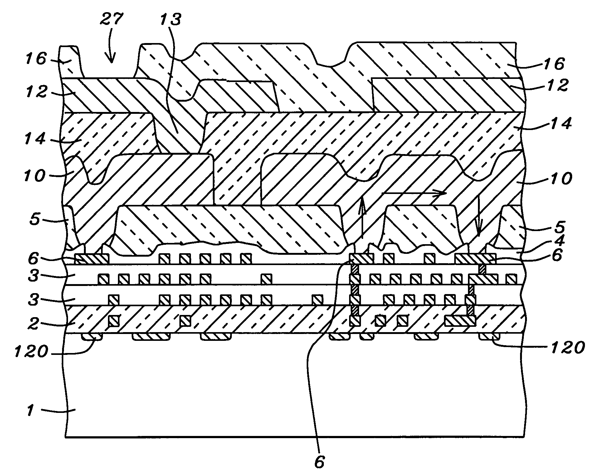
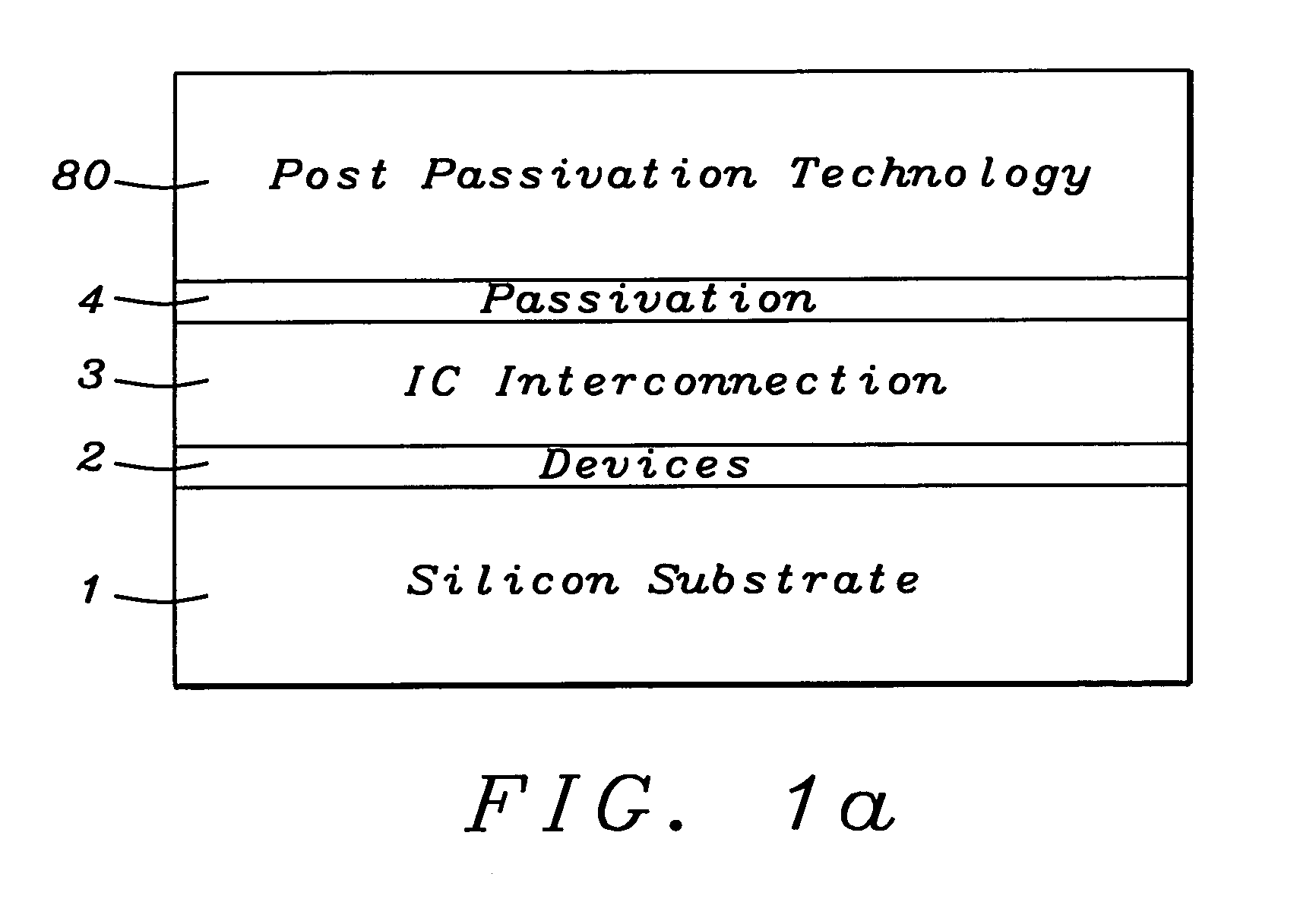
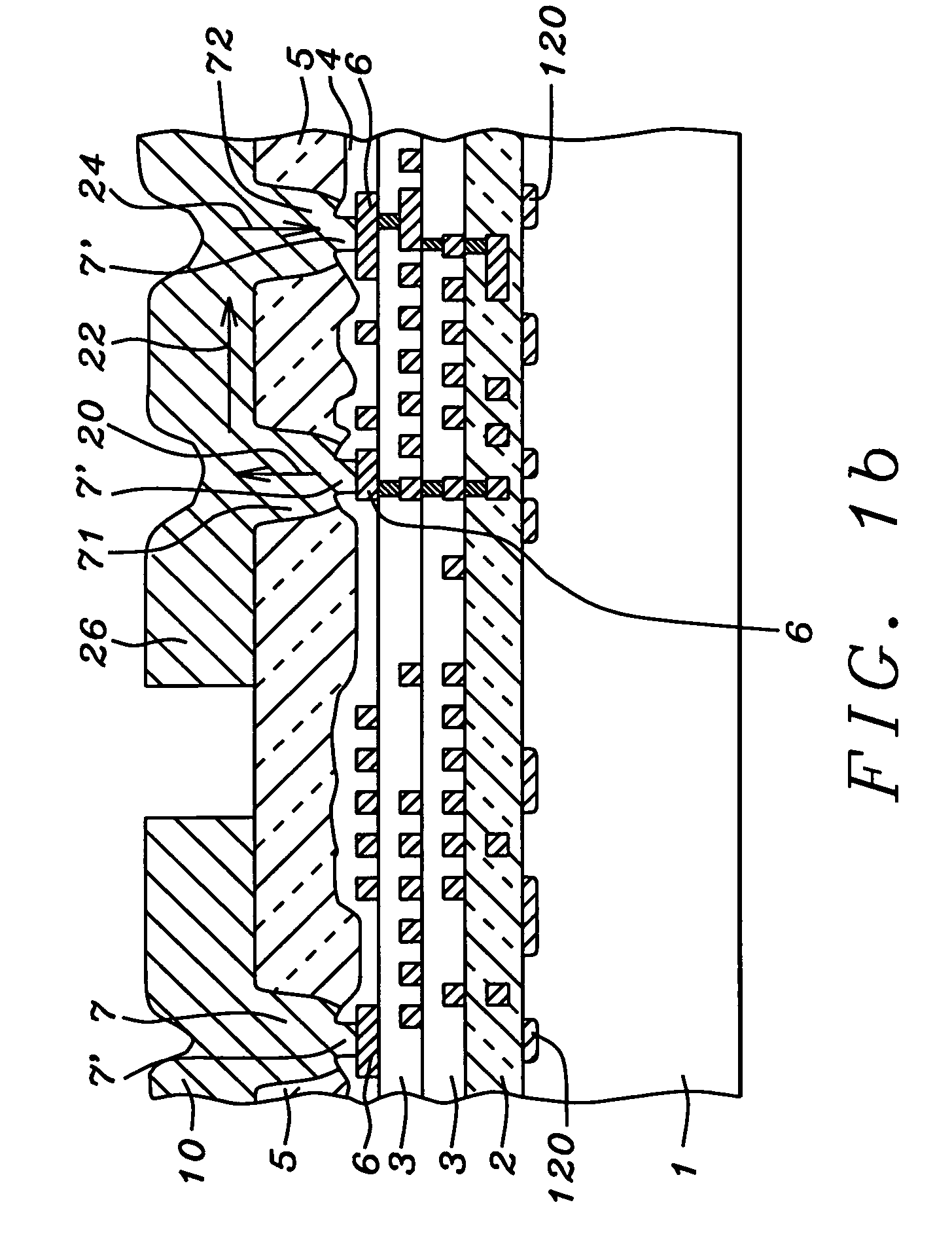
[0044]The present invention teaches an Integrated Circuit structure where key re-distribution and interconnection metal layers and dielectric layers are added over a conventional IC. These re-distribution and interconnection layers allow for wider buses and reduce conventional RC delay.
[0045]FIG. 1a shows a cross-sectional representation of a general view of the invention. Devices 2 are formed in and on a semiconductor substrate 1, and metallization is accomplished in one or more layers of IC Interconnection 3, above the device layer. These metal layers are referred to as fine line metal interconnections. Typically, the intermetal dielectric (IMD) layers comprise silicon-based oxides, such as chemical vapor deposited (CVD) silicon oxide, CVD TEOS oxide, spin-on-glass (SOG), fluorosilicate glass (FSG), high density plasma CVD oxides, or the composite layer formed by a portion of this group of materials. The IMD layers typically have a thickness of between about 1,000 and 10,000 Angst...
PUM
Abstract
The present invention adds one or more thick layers of polymer dielectric and one or more layers of thick, wide metal lines on top of a finished semiconductor wafer, post-passivation. The thick, wide metal lines may be used for long signal paths and can also be used for power buses or power planes, clock distribution networks, critical signal, and re-distribution of I / O pads.
Description
RELATED PATENT APPLICATIONS[0001]This application is related to Ser. No. 10 / 154,662 filed on May 24, 2002, a continuation-in-part application of Ser. No. 10 / 058,259, filed on Jan. 29, 2002, now issued as U.S. Pat. No. 6,620,728, which is a continuation application of Ser. No. 09 / 251,183, filed on Feb. 17, 1999, now issued as U.S. Pat. No. 6,383,916, which is a continuation-in-part application of Ser. No. 09 / 216,791, filed on Dec. 21, 1998, abandoned, all of which are herein incorporated by reference in their entirety.BACKGROUND OF THE INVENTION[0002](1) Field of the Invention[0003]The invention relates to the manufacturing of high performance, high current, low power, and / or low voltage Integrated Circuit (IC's), and more specifically to methods of achieving high performance of the Integrated Circuits by reducing the capacitance and resistance of inter-connecting wiring on chip.[0004](2) Description of the Related Art[0005]When the geometric dimensions of Integrated Circuits are sca...
Claims
Application Information
Patent Timeline
Application Date:The date an application was filed.
Publication Date:The date a patent or application was officially published.
First Publication Date:The earliest publication date of a patent with the same application number.
Issue Date:Publication date of the patent grant document.
PCT Entry Date:The Entry date of PCT National Phase.
Estimated Expiry Date:The statutory expiry date of a patent right according to the Patent Law, and it is the longest term of protection that the patent right can achieve without the termination of the patent right due to other reasons(Term extension factor has been taken into account ).
Invalid Date:Actual expiry date is based on effective date or publication date of legal transaction data of invalid patent.

