

Printed wiring board and display apparatus
- Summary
- Abstract
- Description
- Claims
- Application Information
AI Technical Summary
Benefits of technology
Problems solved by technology
Method used
Image

Examples
first embodiment
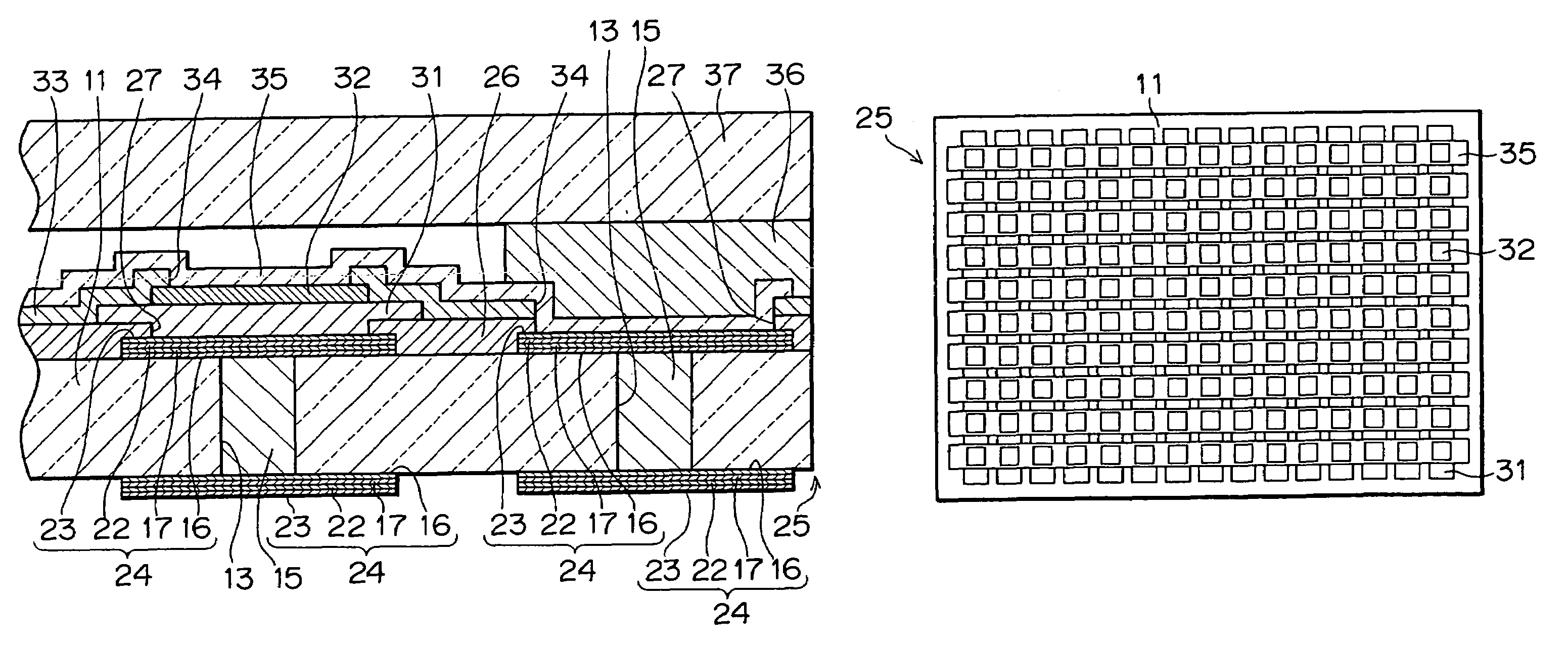
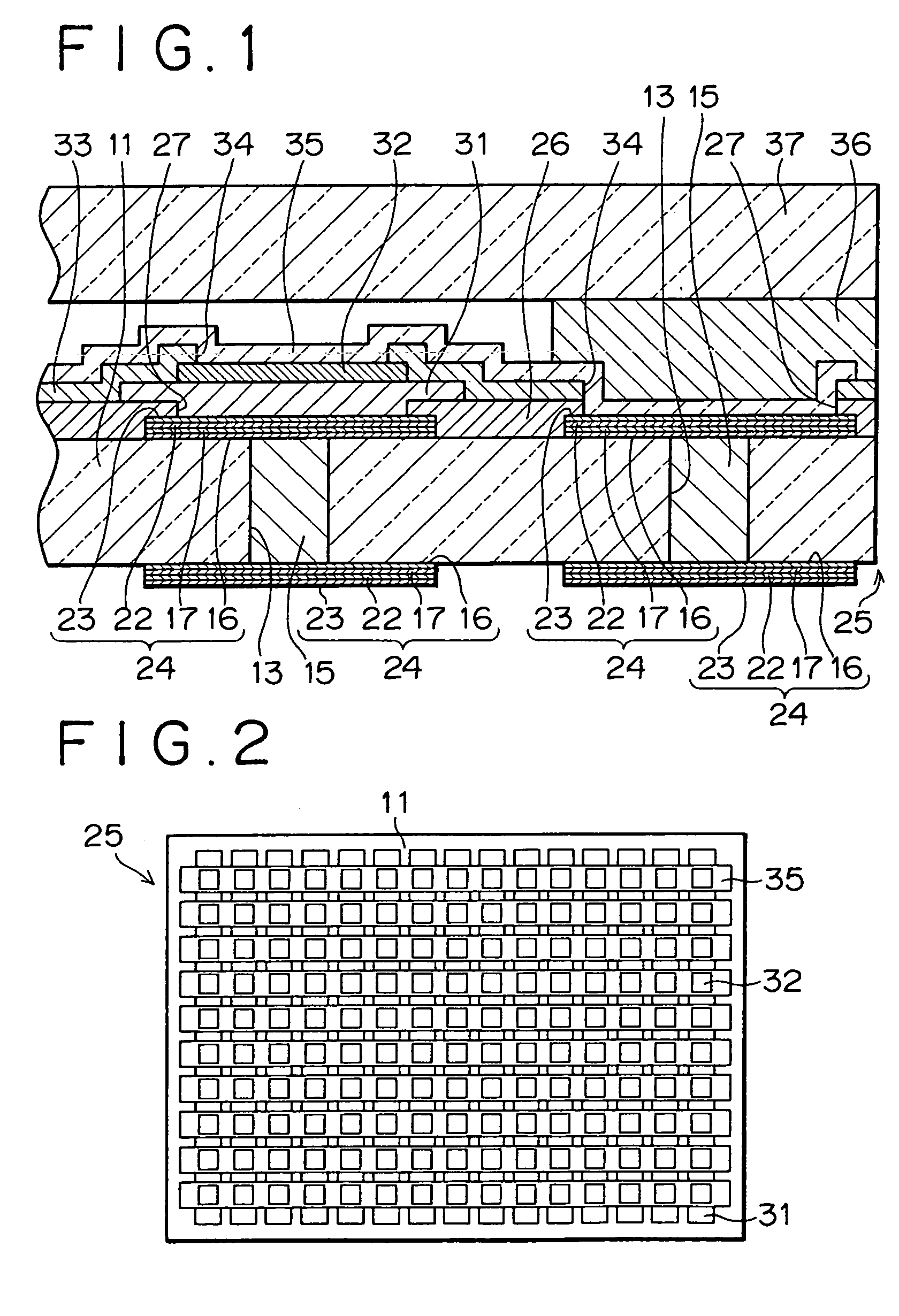
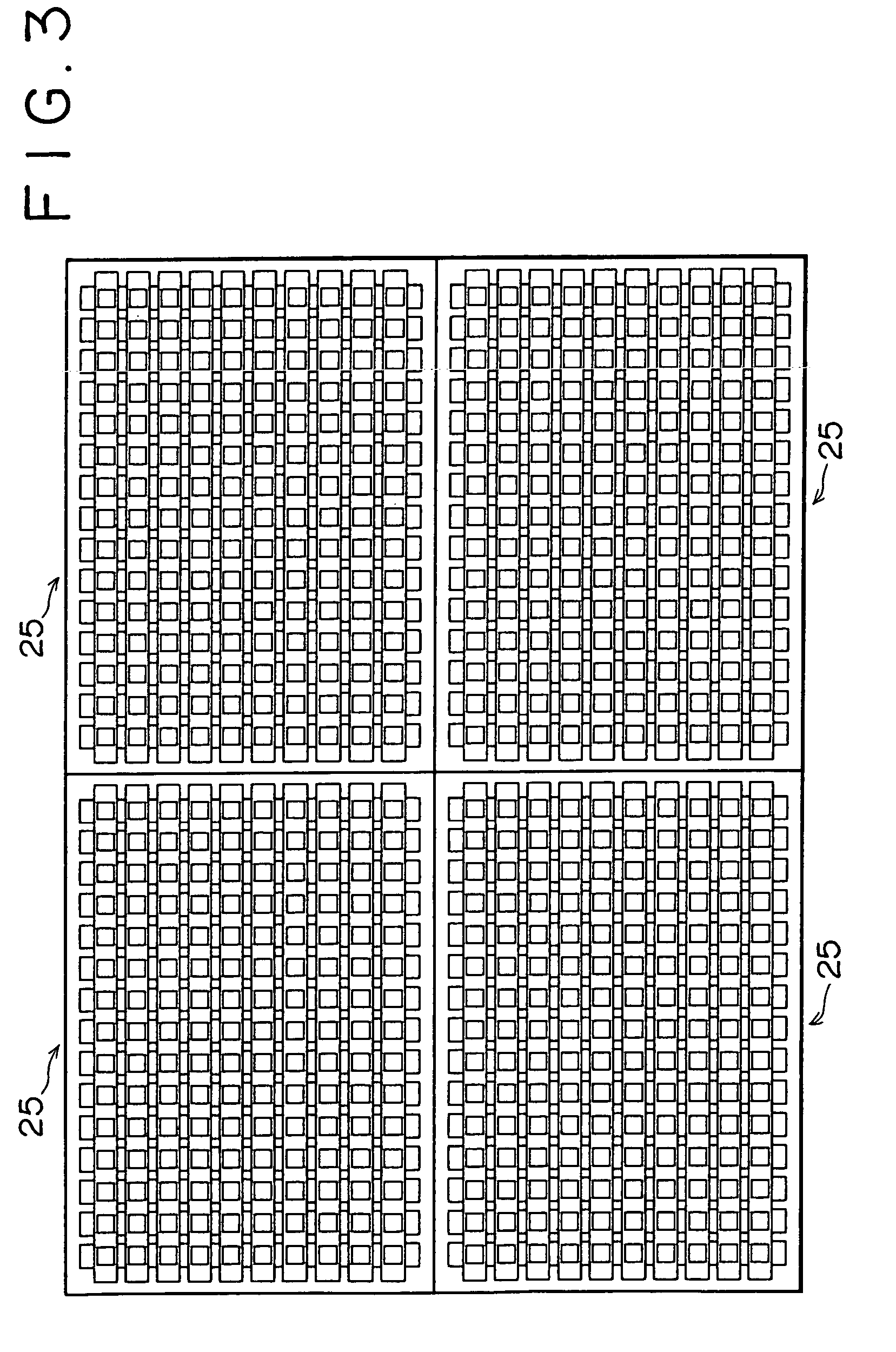
[0031]A method of fabricating a printed wiring board and an EL display apparatus will be described with reference to FIGS. 1 to 6C. As shown in FIG. 4A, a glass substrate 11 of 1.1 mm in thickness made from a no-alkali glass is prepared, and through-holes 13 are formed in the glass substrate 11 at positions corresponding to those of anode electrodes and cathode electrodes necessary for a simple matrix type EL display apparatus by turning a diamond drill 12 or turning the diamond drill 12 while imparting ultrasonic waves to the diamond drill 12.
[0032]The diamond drill 12 is formed by electrodepositing fine particles of diamond on the surface of an ultra-high hardness steel containing typically Cr, Mo, W, Mn, Ni, and Ti, or sintering a mixture of a powder of the ultra-high hardness steel and fine particles of diamond. The frequency and energy of ultrasonic waves are set at about 20 kHz and 500 W, respectively. The turning of the diamond drill 12 with ultrasonic waves imparted to the ...
second embodiment
[0040]A method of fabricating a printed wiring board and an EL display apparatus according to the present invention will be described with reference to FIGS. 7 to 9D.
[0041]First, as shown in FIG. 8A, a glass substrate 41 of 1.1 mm in thickness made from a no-alkali glass is prepared. Epoxy resin films with copper foils are press-bonded on both surfaces of the glass substrate 41 by using hot rolls 42. In this way, an epoxy resin film 43 of 40 μm in thickness and a copper foil 44 of 18 μm in thickness provided thereon are formed overall on each surface of the glass substrate 41. Then, as shown in FIG. 8B, portions of the copper foils 44, located at positions where through-holes corresponding to anode electrodes and cathode electrodes necessary for a simple matrix type EL display apparatus are to be formed, are removed by etching, or the surfaces of the copper foils 44 are overall removed by etching.
[0042]As shown in FIG. 8C, like the fabrication step in the first embodiment shown in F...
PUM
| Property | Measurement | Unit |
|---|---|---|
| Time | aaaaa | aaaaa |
| Electrical conductor | aaaaa | aaaaa |
Abstract
Description
Claims
Application Information